China’s domestic semiconductor industry has had to respond to the challenge of U.S. export controls by working with industrial ministries in Beijing and key local governments, such as in Shenzhen and Shanghai, to move the entire sector up the innovation curve and value chain on a compressed timetable. It is now clear that the immediate localization of the semiconductor equipment sector is Beijing’s top industrial policy priority.
In my November 2024 article for this journal, I noted that “[b]y the end of 2025, we should be in a better position to determine the near and medium-term prospects for China’s semiconductor industry to close some of the technology gaps and overcome some of the identified technological choke points.”1 Now, in 2026, though some areas of China’s technological landscape remain opaque, one thing is evident and that is that the era of Chinese ascendancy in semiconductor manufacturing equipment (SME) has arrived, and it can be expected to have a dramatic impact on the global IT sector by the end of the decade.
Key to the realization of this vision are two competing yet complementary spheres of influence in the semiconductor manufacturing space, one led by Huawei and which includes thousands of affiliated companies, and the other, the traditional SME sector, vying with the Huawei-led system for funding and influence.
In the year ahead, there will be major pressure on both pieces of China’s SME ecosystems to make greater progress on tool development and to begin using more domestic tools for commercial production across a wide swath of technologies. This process is now driven more by U.S.-China competition in artificial intelligence (AI) and the need to eventually replace U.S.-based advanced AI hardware providers Nvidia, AMD, and Intel as part of an effort to develop a fully indigenous AI stack on top of a domestic SME supply chain, one that can scale to meet the requirements for advanced compute hardware. This will require new ways of thinking about innovation, competition, state support, market forces, and international decoupling and dependencies.
While many observers continue to assert, erroneously in my view, that “China has always aggressively pursued self-reliance,” the semiconductor industry has, in fact, been very different from other sectors, with global supply chains and tool complexities that have made it particularly difficult for competitors to jump into the game and gain significant market share, particularly at advanced nodes. Given the need to compete at the cutting edge, Chinese fabs, in the absence of U.S. export controls, would have remained—and to some extent, still do—reluctant to rely on inferior domestic tools. But U.S. controls, particularly the October 2022 package, have added rocket fuel to domestic tool makers’ attempts to break into leading fabs in China. This means that, by 2028, even without Chinese government support, every new fab in China will likely be able to operate with 50 percent of its tools being domestic made, something that would have been inconceivable in 2022.2 As we will see, Chinese toolmakers are reaching the frontier faster, developing substitutes, and competing formidably in global markets.
The issues discussed in this paper remain sensitive in China, with guidance in 2024 from the Chinese Semiconductor Industry Association (CSIA) to members to be careful conversing with foreigners about the industry. This year, the Ministry of Commerce (MOFCOM) also put the publication Tech Insights on its Unreliable Entities List (UEL)3 for its reporting on Huawei semiconductor designs being manufactured at TSMC via a third party. These actions, coupled with unlisted companies, select media leaks, and renewed focus on the details of arcane subjects like advanced lithography by non-experts, make it harder than ever to get under the hood and over the noise to assess progress.
Against this backdrop of increasing opacity and complexity, the goal of this paper will be to provide realistic and well-sourced assessments of how China’s semiconductor industry, from government planners to individual companies, is reacting in a world of U.S. export controls and heavy demand for advanced compute capacity.
Between DeepSeek and Huawei: Beijing’s Funding Priorities
A key challenge for Chinese industrial policy lies in determining how to support the broad semiconductor industry while also giving domestic technology giant Huawei enough room to lead innovation. Huawei is at the center of an ecosystem that includes roughly two thousand companies across the semiconductor supply chain, as well as about thirty organizations working on advanced lithography. Together, these firms are attempting to achieve technological breakthroughs in areas long considered strategic “choke points,” especially those targeted by U.S. export controls. The goal according to Huawei founder Ren Zhengfei is roughly 70 percent self-sufficiency by 2028,4 as part of Huawei’s “Spare Tire/Backup Plan 2.0.”5
For the first time among those watching these issues closely, the technological “choke point” strategy adopted by U.S. authorities across the late 2010s and early 2020s has now been shown to have failed, as Chinese government and R&D officials, as well as key state-backed and private sector firms, have been able to respond to the challenge forcefully and effectively. Leading the response are key policymakers: Vice Premier Ding Xuexiang, and the semiconductor team at the National Development and Reform Commission (NDRC), overseen by Vice Minister Xiangli Bin. A new AI-focused group at the NDRC overseen by Vice Minister Huang Ru is also increasingly important, as semiconductor and AI-related industry policies increasingly dovetail.6
No one in China now thinks of semiconductors as in any way separate from progress in AI, and there is an increasingly symbiotic relationship between AI hardware manufacturing and design leaders (e.g., Huawei, CXMT, YMTC, Cambricon, XMeta, Enflame, Sophgo, and Biren) and AI model developers (e.g., DeepSeek, Alibaba, Tencent, Baidu, ByteDance, and more). Intermediaries and second-tier cloud platforms including Infinigence and SiliconFlow, plus major research players such as the Shanghai AI Lab, also factor into this nexus.7 This convergence was particularly evident at the World AI Conference (WAIC) in Shanghai in late July 2025.
Vice Premier Ding is the most senior official responsible for overseeing China’s semiconductor industrial policy and serves as the central political authority for major technology and industrial decisions. His continued influence in 2026 signals strong backing for the current strategy, which includes preserving Huawei’s leading role in shaping large segments of the semiconductor ecosystem; the Chinese tech champion now exerts significant influence across critical supply chain inputs and core technologies. This role, however, is both indispensable and controversial. While Huawei has become a focal point for national efforts to overcome U.S.-imposed technological choke points, other firms in the sector are wary of its expanding dominance.
Leading domestic foundry SMIC, for example, has faced pressure to manufacture Huawei’s most advanced chip designs by stretching existing foreign equipment to its limits. This includes deep ultraviolet (DUV) lithography systems supplied by the Dutch firm ASML, which are being pushed beyond their intended capabilities, often resulting in low and inconsistent yields. The urgency stems from Huawei’s need for system-on-chip (SoC) processors for its consumer devices—especially smartphones, as well as for advanced AI chips in its Ascend 9XX series.
Opposition to the Ding–NDRC–Huawei nexus has emerged from other bureaucratic actors, particularly the Ministry of Industry and Information Technology (MIIT). MIIT oversees the National Integrated Circuit Industry Investment Fund, also known as “the Big Fund,” which is now in its Phase 3, with 344 billion RMB (US$47 billion) in capital “directed . . . squarely at accelerating the domestic chip ecosystem.”8 The ministry and the Big Fund support a broad range of semiconductor firms and are concerned that Huawei has been granted excessive influence over the domestic ecosystem.
The Big Fund itself faces challenges. Disbursement under Phase 3 has been slow, as officials remain cautious in the wake of earlier corruption scandals. Ding’s office, formally established only last year, took time to consolidate authority, reflecting significant internal bureaucratic wrangling before it emerged as the de facto coordinating center for semiconductor policy.
Phase 3 was similarly delayed while central authorities restructured oversight mechanisms following past scandals and reassessed strategy. This reassessment contributed to the current approach: a Huawei-centered model supported by Ding and the NDRC, with the Big Fund playing a complementary role.
A further institutional development occurred in late 2025 with the launch of the National Venture Capital Guidance Fund, which is ultimately intended to mobilize a much larger sum of capital than the Big Fund: up to 1 trillion RMB (US$144 billion). Controlled by the NDRC and partially overlapping in mandate with the Big Fund, this new vehicle is designed to invest early, modestly, and for the long term in “hard tech” sectors, including semiconductors and artificial intelligence. According to a Ministry of Finance official, its investment horizon extends fifteen to twenty years, signaling a shift toward more patient capital in support of strategic technological development.9
After its establishment, Ding’s office was initially slow to issue formal directives. This hesitation likely reflected an effort to clarify its relationship with the Big Fund and to coordinate more effectively with regulatory bodies such as the China Securities Regulatory Commission (CSRC), particularly in exploring how capital markets could better support semiconductor development. In practice, however, many of the core policy initiatives were already in motion before the office became fully operational. More broadly, there has long been a perception within the system that the Big Fund operated with considerable autonomy, while MIIT pursued its own agenda, resulting in limited cross-government coordination. Early on, some observers questioned whether Ding’s office was exercising sufficient authority to align these competing bureaucratic actors, including MIIT.
As 2026 proceeds, that dynamic appears to be shifting. Ding and the NDRC are becoming more assertive and visibly engaged in coordinating policy. They continue to back Huawei as the central actor overseeing major segments of the semiconductor ecosystem, although Ding’s formal mandate extends well beyond any single firm and encompasses the broader strategic direction of the industry.10
Even as policymakers in Beijing debate the industry’s direction and the Big Fund reassesses its priorities, Huawei has been moving ahead with its own strategy. The company is systematically developing a large-scale semiconductor manufacturing complex in Shenzhen, securing equipment and tooling through multiple channels. If this facility reaches commercial-scale production at advanced nodes—currently understood to mean 7 nanometers, potentially as early as this year—some industry observers expect a significant shift. In that scenario, Huawei could scale back its reliance on SMIC and transfer most, if not all, of its advanced chip production to its Shenzhen fabrication cluster.11
The establishment of Huawei’s new manufacturing complex has been difficult and disruptive. It has also generated unease within more established segments of the semiconductor industry. The effort reportedly involves aggressive talent recruitment and strong political pressure, reflecting Huawei’s backing from the NDRC, Vice Premier Ding, and ultimately Xi Jinping himself. Xi appears to view Huawei as the actor most capable of delivering critical technological breakthroughs. By contrast, the Big Fund has struggled with corruption scandals, bureaucratic inefficiencies, and uneven results. In the eyes of some policymakers, its shortcomings contributed to a lack of genuine innovation, leaving Chinese firms exposed to U.S. export controls and other external pressures.12
The emergence of Chinese AI model developer DeepSeek in early 2025 has also had a profound impact on the entire technology space in China, including all the way down the technology stack to semiconductors.13 The issue was highlighted by DeepSeek’s V3 and R1 models around access to sufficient numbers of advanced GPUs amid evolving U.S. export control policies in the second Trump administration. With Beijing signaling that AI development is now a priority issue for economic growth, firms in China across the AI stack are on official notice that they must make progress to reduce dependence on foreign sources of key technology inputs, as competition with the United States intensifies. The urgency of this priority was underscored by President Xi’s meeting in February 2025 with private sector tech leaders including Huawei founder Ren Zhengfei and DeepSeek CEO Liang Wenfeng, a rare event in Chinese public life.14 There is no going back, and AI is front and center; no one is talking as much about 5G/6G, biotech, or other potential areas of competition.
Thus, the semiconductor industry, and by extension the AI sector in China, is now in a multiyear transition period, with multiple trends unfolding at once, including intense investment in domestic tools and supply chains and continued use of a large suite of foreign SME tools. These include DUV immersion lithography systems and memory-focused tools from Japanese suppliers that are enabling progress in the advanced memory architectures needed for AI, such as high bandwidth memory (HBM). All of this is preparing for the moment that Huawei, SMIC, and other foundries can field nearly all domestically developed node processes, free of any constraints imposed from Washington or other allied capitals.
One industry insider told me that the transition from foreign to domestic tools in China was the “largest unforced technology transfer in history.”15 In addition, a key corollary of this process is that the gains in domestic toolmaker capabilities derived from experience in memory production, which is somewhat easier than for logic, will eventually be ported over to the logic stack. The day in which Chinese firms are fully free of U.S. technology and U.S.-imposed constraints is still quite distant, but Ren’s notion of 70 percent self-sufficiency by 2028 is certainly attainable in some but not all areas: the groundwork is currently being laid to surpass that number.
All of this is occurring on a timetable absolutely inconceivable to anyone working in the Chinese semiconductor industry before October 2022, including U.S., Dutch, Japanese, South Korean, and Chinese engineers and company officials. Before this key inflection point, the latter would have considered such a course both undesirable and impractical. Yet that course is well underway.
The Challenges Facing Advanced Node Manufacturing
In assessing the current state of advanced node production in China, it is useful to start within what might be called the “traditional” SMIC Semiconductor Industrial Complex (SSIC). Establishing this baseline is essential before turning to the more opaque and significantly more complex ecosystem emerging in early 2026 under Huawei’s direction; visibility in the “rebel” Huawei Semiconductor Industrial Complex (HSIC) is far more limited. Unlike SMIC, which is publicly listed, Huawei remains privately held. As a result, key milestones are closely guarded by Beijing, the NDRC, and Huawei headquarters and media reports are not wholly reliable: for instance, a December 2025 report by Reuters claiming to shed light on the facilities and workings of the HSIC was replete with false names and secure entry systems.16
The HSIC remains, in many respects, a “complex in embryo,” but it is advancing rapidly toward the targets articulated by Ren Zhengfei. At times, this progress appears to come at the expense of the traditional SMIC-centered system. There are also points of overlap and cooperation between the two ecosystems. While Ren’s broader vision likely encompasses the development of the entire domestic semiconductor industry, much of the practical experience and capability at the most advanced nodes may ultimately consolidate within the Huawei-led complex.
SMIC has made considerable progress on advanced node production since 2022. This is partly because of the firm’s ability to leverage well-known techniques, such as quadruple patterning.17 That said, SMIC faces intense pressure given the scale of domestic demand for advanced-node semiconductors. Its core advanced manufacturing base remains the SMSC facilities in Shanghai, where two fabs—SN1 and SN2—are configured for 7 nanometer and below production.
At present, SMIC continues to rely on ASML deep ultraviolet (DUV) lithography systems for 7 nanometer and limited 5 nanometer output. At the same time, it is expanding capacity across other parts of its production lines using qualified non-U.S. equipment, including a combination of Chinese and Japanese tools. Based on available indications, SMIC appears to have secured enough ASML DUV systems to scale advanced-node production to roughly 70,000 wafers per month, with approximately thirty-five thousand wafers per month capacity at each of the SN1 and SN2 facilities.18
Domestic toolmakers have developed etch, deposition, clean, and metrology tools to work well with multipatterning lithography. It is likely that SN1 reached this full thirty-five thousand capacity in 2025. In 2026, given tool use, increased domestic inputs, and some mature node capacity coming online at the Hua Hong and Huawei fabs, total capacity could be close to a hundred thousand wafers by the end of 2026.
If, as analyst TP Huang has noted,19 we assume a hundred thousand wafers with thirty good dies per wafer would translate into three million AI semiconductors per year, this would represent the upper bound on production of the combination of Huawei Ascend and other advanced GPU designs from smaller players. If all the advanced tools available to SMIC are used for AI processors, the number here could be much higher.20 Yet SMIC must also produce SoCs for smartphones from Huawei. In the mix also are DDRx and HBM, where Chinese leaders CXMT, Fujian Jinhua, SwaySure, and YMTC will ramp up production in 2026.
The key issue then for 2026 is how SMIC will allocate this capacity between Huawei, with its Ascend, Kunpeng, and Kirin processors, and the many other capable domestic GPU designers. As of late 2025, it appears that SMIC agreed to allot a limited amount of its production capacity to Chinese GPU design firms, such as Biren, MetaX, Enflame, Moore Threads, and Sophgo, that were added to the U.S. Commerce Department’s Entity List over the past two years and are prevented from using TSMC to manufacture their designs. SMIC will devote more capacity to these startups in 2026, as many of them have gone or will go public via blockbuster IPOs; Moore Threads and MetaX did this in late 2025 and Biren in early 2026.21 Device and automaker Xiaomi, on the other hand, is still able to use TSMC to manufacture its smartphone SoCs at 3 nanometers. These designs include GPUs, taking even further pressure off SMIC and allowing other players, such as ZTE, to use advanced ASIC SoCs from Qualcomm for their smartphones.22
Complicating attempts to assess SMIC production capacity at both 7 and 5 nanometer-class nodes is the issue of third-party players being used for production of said nodes at TSMC, based on Huawei and other designs. A report by industry publication TechPowerUp in December claimed that SMIC has “officially achieved volume production of its newest 5 nanometer-class node called SMIC N+3,”23 but rumors were circulating in China at this time that any real 5 nanometer production was actually coming from third-party sources using TSMC to produce designs. As of early 2026, there were no clear teardowns of actual Chinese products likely to be using a 5 nanometer part manufactured at commercial scale at SMIC.
In another report by the Financial Times in August 2025, the claim was made that “China seeks to triple output of AI chips to boost DeepSeek ambitions.”24 This report has some issues—in part because it is based on some assumptions about how SMIC’s advanced node capacity will be supplemented next year by new output from Huawei’s fabs in Shenzhen and Dongguan. Estimating when these facilities are likely to be online and conducting high-volume production is far more problematic than for SMIC, a known quantity, with known limitations in terms of tool access and a more predictable track record on pushing tools like DUV to their limit through techniques (e.g., multipatterning).
Before moving on to the HSIC, it is worth touching briefly on the memory situation, because this is critical to assessing outputs of Huawei’s Ascend and other GPU systems by SMIC in 2026.
Progress in China’s Memory Sector
As of 2026, ChangXin Memory Technologies (CXMT) is the only mainland Chinese firm with a broadly evidenced path to producing meaningful quantities of high-bandwidth memory (HBM). The most defensible expectation, however, is that output will be concentrated in earlier-generation HBM (HBM2/HBM2E) and limited early-ramp HBM3 rather than internationally competitive HBM3E at scale.25 Some industry observers describe a staged progression from initial HBM2 capability toward HBM3/HBM3E, but they also underscore why moving up the HBM stack is yield-compounding and process integration-intensive in ways that quickly expose any immaturity in underlying DRAM process technology or back-end assembly control; this is owing to challenges with through silicon vias (TSVs), bonding, thermal, and test.26 CXMT’s roadmap accounts for the lack of American SME. CXMT has been unable to access US SME since January 2025, when the United States tightened the parameters of its end use controls on DRAM and HBM, making CXMT a key incubator for domestic equipment companies.
Reporting by Reuters across 2024 and 2025 similarly indicates that Chinese firms (including CXMT) have been working to secure equipment and develop HBM; the same source suggests that CXMT has ambitions to begin mass production of HBM3 in 2026 alongside investment in dedicated HBM packaging capacity in Shanghai.27
For YMTC, 2026 is better framed as an “option creation” year for HBM rather than a year of delivered volume. YMTC’s core franchise remains 3D NAND, and the strongest public evidence for a HBM pivot is Reuters reporting that YMTC is planning to enter DRAM manufacturing, including advanced variants relevant to AI chipsets, after Washington expanded restrictions affecting the advanced memory supply chain.28 Even if that plan translates into project execution, the critical work in 2026 is likely to be front-end DRAM learning and early integration trials (cell and periphery process stability, yields, then TSV stack, and test flows), not competitive shipments; the empirical base for forecasting large YMTC HBM volumes in 2026 is therefore thin relative to CXMT. 29 YMTC’s work has proceeded without U.S. tools since 2022, when it was added to the Entity List and end use controls were imposed on NAND, blocking all U.S. equipment and servicing of existing inventory.
Otherwise, SwaySure’s relevance to China’s prospective HBM supply in 2026 is principally ecosystemic and policy-linked, rather than demonstrated through transparent product benchmarks. Media sources have described SwaySure as part of a Huawei-associated semiconductor network considered for U.S. trade restrictions, and SwaySure was subsequently placed among entities targeted in the December 2024 export control expansion announced by the U.S. Commerce Department.30 Those actions and the underlying Entity List framework imply that U.S. authorities view SwaySure as materially connected to advanced semiconductor capacity development, but public reporting does not provide the same level of technical specificity, such as node, stack height, qualification status, sustained output, etc., that would support high-confidence estimates of SwaySure-origin HBM volumes in 2026. Industry sources indicate that SwaySure remains within the 14 to 28 nanometer logic integrated circuit (IC) range, a relatively profitable node with an abundance of local and international tool offerings.
Across all three firms, judgments about HBM capacity growth in China in 2026–27 are often overstated for several reasons: they conflate front-end DRAM wafer capacity at HBM-suitable nodes; back-end HBM stack assembly capacity—though silicon via (TSV) formation, wafer-to-wafer or die-to-wafer bonding, chemical mechanical planarization/polishing (CMP), metrology, test; and sellable, qualified HBM output after yield loss across the full stack.31 The most credible capacity assessments therefore start from hard signals (e.g., verified fab buildouts, tool deliveries, and third-party reporting of concrete ramp intentions) before applying conservative haircuts for yield-compounding, equipment chokepoints, and qualification timelines. Trend Force reporting on China’s HBM efforts illustrates the tendency toward ambitious “target” dates, such as HBM2 by 2026, while also acknowledging the gap to incumbents; this gap is precisely why 2026–27 projections should be anchored on demonstrated shipments and customer qualification rather than nominal installed capacity or aspirational roadmaps.
Evaluating the Huawei Semiconductor Industrial Complex
Given all the moving parts, including the memory sector, assessing where HSIC is with respect to specific tool capabilities is complex, with media hype, industry rumors, and outright disinformation clouding the picture.32 There are several different trends among key toolmakers deeply embedded in the HSIC.
First, a complex game is currently being played out. SMIC has buckled under pressure from central authorities to devote a majority of its advanced node capacity to Huawei for its Kirin, Kunpeng, and Ascend processors. There is also increasing animosity toward Huawei within the industry, which stems from Huawei’s power and the fact that its companies are poaching engineers from other parts of the industry to work within the HSIC.
In terms of producing Huawei’s designs, SMIC faces challenges in terms of yield. Huawei’s Ascend series in particular requires large complex dies, and yields remain low. But SMIC has a major advantage in terms of scaling up capacity for advanced nodes, before Huawei will be able to bring online significant capacity at 14 and 7 nanometers and below. Huawei’s fab efforts, including two facilities in Shenzhen and one in Dongguan, are using some ASML lithography tools shipped in 2023–24, purchased via various channels, including likely through some third-party cutouts.33 But the firm, unlike SMIC, is also working on validating domestic extreme ultraviolet lithography (EUV), likely at Shenzhen or Dongguan. It is difficult to determine how close Huawei efforts on EUV are to reaching some level of stability (this issue will be tackled separately below).
Several companies are central to supplying the Huawei fab complex in Shenzhen; these companies will eventually also supply the Dongguan EUV fab effort. SiCarrier is one of those key players, but claims coming via the media about SiCarrier can be difficult to evaluate. For example, an October 2025 story featuring claims about semiconductor design software being touted by SiCarrier were misleading.34 The software was a PCB design tool and is far from critical or filling any existing gap.
Expectations within the Chinese semiconductor industry had been running high ahead of the exhibition where SiCarrier was scheduled to make its announcement. Rumors had circulated widely that the company might unveil a major breakthrough, possibly related to EUV. Adding to the anticipation, a Shenzhen government official released a video that quickly went viral, suggesting that SiCarrier would deliver a significant surprise. Even accounting for the Shenzhen government’s strong backing of the company, it was highly unusual for a public official to preview a firm’s forthcoming product developments. As a result, when the announcement fell short of the elevated expectations, particularly regarding EUV progress, the sense of disappointment at the event was immediate and pronounced.35 Following this, SiCarrier has been able to include a legitimately advanced tool into its EDA portfolio, namely Design for Test (DFT), a specialized category within EDA (Electronic Design Automation) toolchains that focuses on making ICs easier to test and debug after fabrication.36 According to industry observers, this capability was designed by HiSilicon.
This episode illustrates several major new trends within China’s semiconductor industry. Here, SiCarrier is expanding into EDA tools and working with Huawei’s HiSilicon, a formidable reservoir of engineering expertise, particularly for semiconductor design and EDA tool expertise. HiSilicon likely has full access to the source code of one of the major EDA tool vendors. It appears that SiCarrier is being redesigned to be both an equipment maker and EDA tool player; it could potentially play a role in IP also.37 The Huawei fab where tools are being tested from SiCarrier is Pengxinwei (PXW), also funded by the Shenzhen government and added to the Entity List in December 2024.
The close symbiotic relationship between SiCarrier and PXW, both having access to former Huawei engineers and technology injects, will be critical to the ultimate success of the HSIC to get to commercial levels of sustained production below 7 nanometers. At the same time, there is considerable criticism of SiCarrier coming from within the industry—and by extension, Huawei. One commentator, writing in October of last year after a major industry exhibition in Shenzhen, had been highly critical of the hype around SiCarrier, accusing the firm and the Shenzhen government of colluding to pump up the future value of the stock with misleading claims.38 This was a highly unusual situation, with such pointed criticism of both Huawei and a major city government coming without any apparent censorship from the authorities.39
It is likely that SiCarrier is providing many other tools for a domestically produced EUV production line. SiCarrier is focused only on nodes at 7 nanometers and below and claims to have tools in most advanced fabs in China,40 either in production or being qualified; these include SMIC, Hua Hong, YMTC, and PXW.41 This is likely the case at Huawei’s Dongguan advanced production facility as well. As of late 2025, the best assessment that can likely be made is that SMIC will be able to competently manufacture something similar to N6 or N7+; the HSIC is likely to struggle into 2026 to get anything near commercial yields first for a 14 nanometer production line, while then moving to a process similar to N7. SMIC’s N+1 or N+2 processes, which are DUV-based with limited multipatterning, achieve transistor density and power/performance roughly in the same class as TSMC’s early EUV–era nodes.
These are not identical in tooling or EUV usage, but the circuit density and performance per watt are approaching the same range. Here, HSIC/PXW appears to be targeting 14 nanometers with an N7-like process, which implies that the HSIC is trying to establish a mature DUV production line at 14 nanometers, likely as a steppingstone toward 7 nanometer class capabilities by roughly 2026. Yet yield, defect density, and reliability remain challenges. The Shenzhen-based fab run by PXW is eager to commence some commercial production and will buy, repurpose, refurbish, or build tools to achieve this goal, according to industry observers.42
For now, however, the splitting of the domestic industry into HSIC and SMIC-led blocs appears to be progressing further. SiCarrier represents an aggressively promoted, government-backed entrant aiming for a “Huawei-style full-stack” semiconductor equipment ecosystem. Nonetheless, its claimed scale, revenue, and client base remain unverified, and advanced etch capability still resides with AMEC, with Naura dominant in deposition and thermal tools. SiCarrier’s strength today appears mainly symbolic and strategic, not yet technically or commercially proven. This dynamic obfuscates the EUV picture as well.
Wei Shaojun, director of the Institute of Microelectronics at Tsinghua University, said, “This is not only a technological breakthrough, but also a reconstruction of the industrial ecology.” Wei highlighted as well how the Shenzhen model—represented by SiCarrier and consisting of government fund guidance, market-oriented operation, and global talent introduction—is rewriting the global semiconductor equipment competition pattern. Equipment manufacturers need to be wary of the trap of “emphasizing R&D over ecology.”43 Only by building a complete industrial chain collaboration system can they truly achieve independent control.
The State of Advanced Lithography: Connecting the Dots
But where is progress on EUV? This is a question I am often asked, and it remains one of the hardest to answer with any sense of fidelity, as of early 2026. Part of the challenge here is that any serious EUV effort will require many other inputs and tools to make itself commercially viable. A light source is important but only as part of a much broader and more complex story. For example, etching is as or more important for advanced three-dimensional structures such as gate-all-around (GAA) designs than lithography.
There are multiple efforts afoot within the system in China to reach something resembling EUV. (Admittedly, much of the detailed information on EUV progress in China remains tightly held, though that is likely to change in late 2026 or early 2027.) First and foremost, Chinese-language sources describe a critical consortium of players under a broad “national team” umbrella as driving the primary line of development for EUV, which has been given the code-name “Mt. Everest,” reflecting the high degree of difficulty involved. The group has Huawei in the pole position, with the Changchun Institute of Optics, Fine Mechanics and Physics (CIOMP) as a critical coplayer. The overall effort is reportedly supported by “5 companies” and “4 state owned enterprises.”44 Analysis of Chinese sources suggests that these five companies are toolmakers Naura, AMEC, SiCarrier, SMIC, and YMTC; the four SOEs are likely associated with China’s defense industrial complex.45
The team working under the HSIC has moved from a single focus on the light source to putting together a prototype full-scale tool, utilizing parts from other ASML tools. This is very difficult since no spare EUV systems are at hand to cannibalize. It is highly likely that the team described in the December 2025 Reuters report has been able to generate some level of EUV light using LPP (laser-produced plasma), though industry observers have not seen any independent proof that this is accurate; the bulk of the system’s key pieces remains a work in progress.46 The development of this system appears geared toward putting the EUV prototype into a trial production line setting, employing tools from other key players in the HSIC, including but not limited to SiCarrier, which will likely provide the etch and deposition pieces.
There is still an effort being pursued in parallel by at least three competing architectures: the LPP path using an ASML-like approach which hinges on drive-laser power scaling and reliability; another LPP path using multichannel fiber lasers where the key unknown is how fiber-laser wavelengths/coupling alter tin-plasma excitation dynamics and spectral purity, potentially increasing parasitic emissions and complicating collector/optics integration; and a revived discharge-produced plasma (DPP) effort evolving toward laser-assisted discharge, or “LDP”-style hybrids. Regarding the latter, historical challenges have centered around power scaling, but a simpler light-transport stack (and therefore lower aggregate light loss) could, at least in principle, make it a “dark horse,” despite lower raw source output.
The Reuters account of China’s prototype describes a scanner-scale system based on firing lasers at tin to generate EUV light (i.e., an LPP-like paradigm), while public rumor-reporting in 2025 has repeatedly floated LDP as an alternative domestic approach, along with other approaches such as a linear accelerator-based strategy. At this point, however, it appears that LPP with molten tin is the most advanced modus for translating light source work into a prototype system.
Overall, the recent Reuters report frames China’s EUV push as a state-backed, security-heavy “Manhattan Project” effort that reportedly leveraged ex-ASML engineers, clandestine recruitment, and reverse engineering to reach a prototype that could generate EUV light (even if it was not yet ready to be incorporated into a production line that could produce finished wafers). This reverse engineering went up to and included reuse of parts from older ASML tools, unlikely for actual EUV-specific parts.
The same account emphasizes the key bottleneck that separates “EUV light exists” from “EUV lithography works at scale”: the full precision chain of source stability, contamination control, reflective optics quality, and scanner-level mechatronics of Western supply ecosystems—notably ASML and Zeiss optics—remains difficult to replicate quickly. A clear increase over the past two years in published research directly related to EUV and LPP light source approaches and optics suggests a focused effort underway and confirms the role of players such as CIOMP.47 Some industry observers believe that a type of EUV prototype has been “complete” for almost two years and was handed over to SiCarrier a year ago with the idea of putting together the complete process flow, using domestic tools for the other key pieces. This represents the most optimistic view of progress on EUV.48
From a systems perspective, the parts of a DUV scanner that can most easily be cannibalized are the wavelength-agnostic platform modules: wafer and reticle handling, automation and interlocks, precision stages and vibration isolation concepts, thermal conditioning, and the software-diagnostics-calibration infrastructure that turns a complex tool into a replicable manufacturing system. What is least reusable is the photon path. DUV relies on transmissive lens-based optics, while EUV operates at ~13.5 nanometers and requires multilayer reflective mirrors and an overall architecture built around vacuum and contamination sensitivity.
That distinction is why the most technically difficult integration surface in EUV is source-to-collector and illumination-to-projection mirrors, not the factory automation around it. Mainstream EUV concepts rely on LPP (commonly tin-based) for EUV generation and must manage contamination that can rapidly degrade projection mirror performance; practical EUV implementation therefore treats contamination management and mirror protection as first-order design constraints.
Where former ASML engineers, as cited in the December 2025 Reuters report, become most critical then is not in any single component recipe but in end-to-end system closure.49 This phase involves translating overlay, focus, dose, and throughput targets into allocatable error budgets, instrumenting the right telemetry, and running iterative calibration loops that couple stage dynamics, alignment, metrology, thermal drift, and the EUV optical chain into a stable operating envelope. In practice, “making EUV light” is necessary but insufficient; the engineering advantage of ASML is squarely in the integration discipline. This entails control architectures, drift management, and diagnostic methodologies that keep source fluctuations and mirror condition changes from cascading into alignment and overlay loss at production-like operating cycles.
Two of the biggest “missing pieces,” or at least underemphasized enablers, on the road to high-volume manufacturing from a prototype stage are photoresists and defect control. EUV patterning faces well-documented so-called RLS tradeoffs—resolution, line-edge roughness, and sensitivity—and stochastic defect mechanisms (shot noise and chemistry variability) that become dominant as feature size shrinks. These issues can limit yield even when the scanner itself is stable. This is why major patterning suppliers have pushed new photoresist approaches (e.g., dry resist concepts and inorganic, metal-oxide resist directions), explicitly positioning resist as a bottleneck intertwined with overall patterning yield. There is no indication in the Reuters reporting about this critical piece of the equation.
A second set of missing pieces is the broader patterning ecosystem that sits “around” EUV lithography: EUV mask blanks with extremely low defectivity, pellicles that can survive EUV power without unacceptable transmission loss, and inspection to find phase defects—plus the downstream process toolchain of deposition, etch, cleaning, CMP, inspection and process control—are all required to translate EUV images into working devices at a high yield. Industry roadmaps and supplier positioning repeatedly stress co-optimization across these process steps through to final etch and clean; EUV mask infrastructure has long been treated as a commercialization constraint. In other words, an HVM-capable EUV machine is necessary, but advanced node manufacturing is not “just lithography.”
Indeed, a further missing piece not mentioned by Reuters sits upstream of EUV lithography but can become just as binding a constraint as the scanner itself: EUV mask writing. EUV masks are patterned using electron-beam mask writers—increasingly multibeam units—to achieve acceptable write times and control as complexity rises. The global technology leaders are concentrated in a very small set of suppliers: IMS Nanofabrication (Intel-owned) is currently the leading provider of multibeam mask writers, and Intel has explicitly characterized multibeam mask writing tools as “critical” to the EUV ecosystem.
In parallel, Japan’s NuFlare Technology is a major incumbent in mask writing and is marketing multielectron-beam mask writers for advanced nodes, while industry discussions commonly describe NuFlare as a leading supplier of single-beam, variable-shaped-beam mask writers alongside its multibeam roadmap. Here, Chinese domestic firms largely fail to compare: China has a substantial domestic photomask manufacturing base, including firms such as Shenzhen Qingyi Photomask, but publicly available information does not indicate a China-based supplier with production-proven, leading-edge multibeam EUV mask writer capability comparable to IMS or NuFlare.
As a result, if China were to move from an EUV prototype toward an HVM-capable process, mask-writing capacity for EUV masks would most plausibly need to come from at least one of two quarters: installed-base imported e-beam mask writers already in-country plus aftermarket pathways to more, or offshore mask fabrication via non-Chinese mask houses where access is feasible. Export controls, however, are explicitly intended to deny China access to the broader EUV ecosystem and have forced workarounds across multiple chokepoints. The number of patents publicly available related to EUV masks suggests that considerable efforts are being devoted to this critical piece of the puzzle.50
The question remains: what about an actual working EUV tool for HVM? Reuters suggests it will not be reached before 2030. Despite advancements in photoresists,51 etching, and thin-film deposition, Chinese firms in early 2026 still lag behind global leaders in many critical areas that would all need to advance at roughly the same time to enable significant production of GAA architectures. Still, three sets of uncertainties suggest that the timeline to get to a working EUV machine could be sooner than 2030. While some within the HSIC were willing to talk to the media (and details emerged through Reuters), it is possible that progress on all the critical constraint areas—light source, optics, alignment, photoresists, etc.—is moving faster than the article suggests.
In the current era of AI-enabled design tools and data analysis, Chinese engineers may be able to accelerate aspects of the EUV development process. With access to extensive industry knowledge, experience drawn from former ASML engineers, and a growing domestic R&D base in key fields such as optics and advanced materials, they could potentially compress portions of the learning curve that ASML confronted during its decades-long development of EUV lithography. Simultaneously, working against this paradigm are realities of how to gain systems integration experience relevant to EUV and how to make all of the many pieces, only some of which were highlighted above, converge into working scalable production systems that are viable in an HVM environment. Here, there is no substitute for actual experience in a high-pressure production environment.
To this end, it appears certain that there will be an actual 7 nanometer-class fab functioning in Shenzhen; it is likely to become the resting place of the Dongguan prototype that will dovetail with the accumulation of critical experience. Thus, the first priority of the HSIC would be a working advanced node fab running in Shenzhen as soon as possible that can offload production from SMIC and provide Huawei engineers with end-to-end manufacturing capability, drawing on all the elements of the sprawling complex. This will be a critical prerequisite for eventual incorporation of EUV capability since the Shenzhen facility will be a testbed for a new and all-domestic advanced node tool suite, headed by SiCarrier and other domestic tool leaders. Crucially, the most optimistic scenario for EUV depends on the still unverified reporting coming from industry observers that suggests SiCarrier has had the EUV prototype system for a year and is integrating other tools into an end-to-end process (see more on this in the final section).52
Assessing EUV Progress Also Depends on DUV Efforts
Beyond merely assessing EUV progress, the difficulty in understanding the status of domestic efforts to develop immersion DUV systems further complicates the picture; about the only thing certain is that these efforts have picked up substantially since I last wrote on this topic. SMIC, for example, in early 2026, appears to be testing domestic DUV equipment from Shanghai Yuliangsheng Technology Co., Ltd., which appears to be structured as a state-backed joint venture rather than a typical VC-backed startup 53
The firm’s two controlling shareholders are involved in a 50/50 split between SiCarrier and Chuangkewei (Shanghai) Technology. SiCarrier is a critical part of the HSIC and is both linked to and controlled by the Shenzhen municipal government, the Shenzhen SASAC, via Shenzhen state investment platforms. Based on a review of the available sources, Yuliangsheng is providing a domestic 193 nanometer ArF immersion DUV scanner currently in tool validation at SMIC. While the target node is likely 28 nanometers, SMIC does not currently require domestic equipment for the critical layers at its 7 nanometer node, having purchased sufficient ASML systems at SMSC fabs.54 But given SMIC’s experience with pushing ASML immersion DUV systems down to 7 and likely 5 nanometers, this is likely the ultimate goal of this effort.55 Experience gained here will also almost certainly migrate to the Huawei effort in Shenzhen given the involvement of SiCarrier.
At the October 2025 industry exhibition in Shenzhen, another relatively new company in the lithography space also made its debut: AMIES Technology showcased its latest lithography products, including compound semiconductor lithography machines, laser-annealing systems, advanced inspection tools, and solutions for packaging and wafer bonding. AMIES is a spin-off from SMEE and focuses on backend technology related to lithography. SiCarrier is again in the mix, holding 50 percent ownership while SMEE owns the other half. It appears that SMEE will continue to work on dry DUV lithography systems, while another part of SMEE, through the AMIES structure, will be focused on other parts of the lithography business, such as packaging.
Putting all of China’s advanced lithography eggs in SMEE’s basket was obviously no longer tenable, hence the breakup. SMEE had originally been slated to complete the first 28 nanometer DUV system in late 2022 but missed this target by roughly three years, as the first system went to SMIC only in the summer of 2025. Under the new arrangement, it looks like SMEE remains in the lead on dry immersion. Yuliangsheng will take the lead on immersion lithography; it could eventually play a lead role in EUV commercialization. AMIES will then be positioned on the backend, in some sources characterized as an advanced packaging lithography supplier for “packaging steppers.” In August 2025, it reached its five hundredth stepper delivered milestone.
Some reporting indicates that a domestically produced 28 nanometer-class immersion DUV scanner under test at SMIC incorporates a high share of locally sourced subsystems, though the quoted “localization percentage” is definition-dependent and not verifiable from primary disclosures. Reported domestic contributions include an ArF excimer laser light source system associated with Keyi Hongyuan, a dual-stage wafer table subsystem linked to Huazhuo Jingke (described in the secondary reporting as in the 1 to 2 nanometer class, with metric definitions varying) and domestic efforts on projection optics and precision gratings. Public disclosures also show that Chinese suppliers are providing positioning grating components to SMEE, while photomask suppliers such as Qingyi describe 28 nanometer mask work as under development rather than clearly qualified for volume manufacturing.56
Yet what about etch? Given the importance of etch for advanced architectures such as GAA, various tooling systems have to come together at some point to support both DUV and eventually commercial EUV. There are three major etch players in China. First, AMEC has made great strides since the October 2022 U.S. export controls with its flagship ICP/HAR plasma etch (Primo/HD-RIE family), already in high-volume use for 3D NAND/DRAM at YMTC and CXMT (now critical incubators for domestic tools) and marketed/qualified on advanced logic layers. Here, public material claims “5 nm and beyond.” When EUV arrives, AMEC’s selectivity/profile control puts it first in line for critical EUV-adjacent etch.57
Next, Naura currently has the broadest domestic WFE portfolio of etch, deposition, and clean/thermal, with SiCarrier also in that mix. Naura has come to hold substantial domestic etch share, having experienced rapid growth since October 2022. The firm’s tools are already a cornerstone for DUV multipatterning processes at Chinese advanced node fabs.58 Lastly, E-Town Mattson (Mattson Technology China) maintains a niche presence in etch/RTP. The firm’s tools are in some cases present at overseas fabs, but at this point it is not a domestic front-runner for leading-edge logic etch. There were reports in 2025 of a stoppage in the use of Chinese tools at TSMC’s 2 nanometer fabs.59
The U.S. export control regime has had a major effect on the progress being made by companies such as AMEC and Naura. For example, as a result of restrictions on U.S. and Japanese firms, both AMEC and Naura have replaced U.S. sources in key fabs such as YMTC, CXMT, and SMIC, where they have gained considerable experience in production environments that they would not otherwise have accrued so quickly. Instead of dual-sourcing and playing off leading U.S. and Japanese firms, YMTC is managing with AMEC and Naura. YMTC also has a fully domestic advanced NAND line, and their third fab will reportedly be entirely domestic. This has allowed AMEC and Naura to move beyond the copying stage into an iterating stage; production learning has become invaluable and allowed Chinese toolmakers to move faster up innovation curves.
Naura has publicly stated that it has an installed base of three thousand etch chambers, which is quite sizeable.60 At the end of 2024, AMEC had an installed base of more than four thousand Capacitively Coupled Plasma (CCP) etch chambers and 1,025 Inductively Coupled Plasma (ICP) etch chambers.61 This experience will also be critical for the transition to etch for EUV, where both AMEC and Naura might have an edge on SiCarrier.
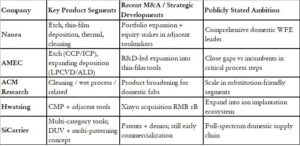
Figure 1: Chinese Toolmakers Moving up the Value Chain as a Result of U.S. Export Controls
Consolidation and Progress: What to Look for in 2026 to 2027
Presently, there is a broader process of consolidation happening across the semiconductor industry tool sector in China (see chart). This process has been underway for some time and appears to be driven from the top, via the NDRC and MIIT. One key factor here will be the degree to which the Big Fund’s Phase 3 will help drive this process. Based on a close reading of Chinese-language sources, we can expect the following types of changes.
Capital will increasingly behave as a force for “platformization.” Rather than funding dozens of subscale point solution vendors, the fund can favor platform primes (multiproduct tool OEMs like Naura and SiCarrier) that can acquire missing modules, teams, or IP—accelerating one-stop domestic capability.
Moreover, deal facilitation, and sometimes deal coercion, will be made via “strategic investor” logic. This is when a transaction is justified as bringing in investors who can provide orders, integration pathways, governance, and political cover—not just money. Lastly, a shift from IPO-led scaling to M&A-led scaling is to be expected. China’s policy environment has periodically encouraged consolidation over scattered listings. The narrative of “merge 200 into 10” is consistent with Phase 3 using capital to reward outcomes that create scale, cross-tool integration, and survivable R&D intensity.
Execution friction will remain high, however, as valuation or ownership disputes and reporting on failed deals are the caution flags: local stakeholders can resist “policy M&A” if it crystallizes losses, shifts control out of the local jurisdiction, or forces unfavorable valuations.
Hence, in 2026, a number of threads will come together to produce further progress in advanced node manufacturing. First, the Big Fund will begin injecting more funding into the tool sectors; while details are scant so far on specific investments for Phase 3, it is clear that there will be targeted investments in semiconductor equipment companies, including 450 million RMB (about US$64.75 million) in Piotech. Recent announcements show investments flowing to companies like Nantong Crystal to boost semiconductor equipment capabilities. Unsurprisingly, the priorities most often mentioned for Phase 3 include lithography equipment and photoresist materials, along with etching equipment, thin film equipment, testing equipment, and cleaning equipment.
More important than the Big Fund though will be the interaction between the SSIC and the HSIC in 2026, centered on DUV and SiCarrier. As important will be tracking how advancements in tools coming out of advanced memory fabs will be integrated into work within both the SSIC and HSIC for advanced logic nodes. These efforts will be happening in parallel, with the NDRC semiconductor group continuing to fund primarily the HSIC, while the Big Fund’s Phase 3 efforts focus on the SSIC and the traditional tool sector. But gains accrue to the HSIC via SiCarrier and its collaborative arrangements with key firms in Shanghai. The Shanghai government and its various investment vehicles will also play a key part in the overall picture going forward, as it is one of the few local governments with substantial capital resources to help fund progress across the semiconductor supply chain.
In terms of progress on AI hardware, the situation is more complex than ever: Huawei and other companies involved in developing memory, packaging, and interconnect roadmaps are under major uncertainty about timelines for some critical inputs, particularly HBM. Still, there is likely to be considerably more progress this year in the memory space than some observers are claiming, but there are complex tradeoffs between advanced tooling at memory fabs, existing stockpiles, and memory requirements for new Huawei Ascend designs and designs of other smaller but fast-growing GPU design firms. Indeed, 2026 will be the year of emergence for China’s HBM capabilities. The entire AI sector globally is memory-limited and the expansion of capacity for HBM in China is coming at a good time in terms of heavy demand for advanced memory that will keep focus and incentives high.
There are two major developments unfolding here. First, Huawei is currently drawing on its stockpile of HBM2E memory chips acquired from South Korean suppliers before the recent surge in AI-related demand. At the same time, the company is working to optimize production yields at SMIC by refining its Ascend chip designs and integrating memory more effectively. Under SMIC’s N+2 process, for example, Huawei faces tradeoffs in developing the Ascend 950; a smaller die size can improve manufacturing yields, but it typically comes at the cost of reduced compute performance. That loss in raw processing power can be partially offset, however, through higher memory capacity and improved interconnect speeds, allowing overall system performance to remain competitive despite process constraints.62
Second, given the major injections of capital coming from the IPOs of CXMT and YMTC,63 increased capex that will benefit mostly domestic toolmakers, and the major investments already underway in memory/HBM capacity, the results in 2026 are likely to surprise. This context will impact the ability of Huawei and other GPU makers to meet demand for more advanced products later in 2026 and beyond.64 U.S. companies, banned from interacting with CXMT and YMTC through a mix of Entity List and end use controls as discussed above, will not benefit from capital infusions at the two companies. This will be a watershed moment for China’s industrial planners and local equipment companies and will be a key milestone for China’s de facto 50 percent localization mandate.
What does all this mean for Chinese AI firms’ ability to source viable domestic semiconductor and software platforms? Could this inflection point portend a real move away from Nvidia and CUDA? While the various pieces are coming together, 2026 will likely not be the year this happens.
Many external observers who seek to demonstrate that China’s semiconductor industry remains far behind, and therefore that export controls are unequivocally effective, often overlook some important factors. First, simple one-to-one comparisons of individual processors are increasingly misleading. Such benchmarks fail to capture broader system-level dynamics. As China’s domestic ecosystem advances in areas such as HBM and system integration, the relative importance of isolated chip performance metrics will continue to decline.65 Second, attempts to prove that export controls work nearly always fail to account for the vast improvements in domestic tool capabilities that will accrue from memory to logic at an increasingly rapid pace.
Again, memory is the poster boy here. CXMT’s sharply improving DRAM sales environment—higher volumes and firmer pricing—creates the operating cash flow and credibility needed to underwrite a step-up into HBM, where the capex and yield-learning curves are materially steeper than in commodity DRAM. In practical terms, stronger “base business” DRAM momentum gives CXMT a larger internal funding pool to run parallel workstreams. They can stabilize or upgrade mainstream DRAM process technology while at the same time financing the incremental R&D, materials qualification, and test cycles required for HBM stacks that must meet AI-grade performance and reliability targets. Reuters framed 2025 as an inflection year for revenue growth, which is precisely the kind of backdrop that can make an HBM push financeable rather than purely aspirational.66
The upcoming Shanghai IPO is the accelerant: CXMT has disclosed plans to raise roughly 29.5 billion RMB (about US$4.2 billion), 67 with proceeds aimed at production line upgrades and advanced DRAM technology development, explicitly including next-generation memory such as HBM. That capital can be deployed to compress timelines in the most bottlenecked segment of the HBM value chain—back-end packaging—where advanced stacking and packaging capability is a gating factor even if front-end wafer output rises. CXMT has said it is building an HBM back-end packaging facility in Shanghai with production targeted to begin by late 2026, positioning IPO proceeds to fund tool purchases, cleanroom buildout, engineering hires, and the long qualification ramp needed to reach meaningful yields and volumes. None of the considerable capital expenditures CXMT is envisioning here are for U.S. tools, highlighting yet again the significant cost to U.S. industry of nonsensical controls on memory.
The outlook is further complicated by several moving parts. These include the potential impact of H200-class GPU purchases on the domestic market; the possibility of third-party production of Huawei’s Ascend processors at TSMC despite tightening controls; the scope for meaningful yield improvements at SMIC, where yields for Ascend chips reportedly remain in the single digits per wafer, with roughly sixty dies per wafer; and the timeline required for the Huawei Semiconductor Industrial Complex (HSIC) to bring advanced capacity fully online. Against this backdrop, Chinese policymakers must weigh a complex array of considerations. These include not only immediate supply needs, but also the pace of domestic progress in HBM, advanced logic, packaging technologies, and software ecosystem development.
In addition, early 2026 will likely see a last-ditch effort by U.S. toolmakers to push policymakers in Washington to consider pulling back some of the late Biden-era export controls, particularly in the memory sector, where DRAM end use controls aimed at slowing HBM development at CXMT were rolled out. This policy push on tools will use an argument similar to the one used for the H200 class GPUs of returning to a sliding scale. Why would H200s produced using a 5 nanometer process at TSMC with HBM3 be allowed for shipment to China if the end use controls from October 2022 are now glaringly outdated?
The absolute approach favored by Biden’s National Security Advisor Jake Sullivan has failed, and there will be a growing chorus in industry and some quarters in Washington to rethink the entire edifice of U.S. export controls.68 The pushback will be strong. Changes in the U.S. controls regime could have a significant impact on China’s memory sector in particular, but the timing and impact are difficult to assess as of early 2026. Ironically, relaxing the controls on SME is the only way the U.S. government can stymie the further development of SME in China.
As part of any reassessment of U.S. policy on SME export controls, the Trump administration may revisit the Trilateral Agreement, which saw a modicum of tool control alignment with the Dutch and Japanese governments. Dutch toolmaker ASML had to reapply for licenses for shipments of DUV equipment and support for its existing installed base in China.69 With no clear policy direction coming from the current National Security Council, the directionality of U.S. policy in this arena as of early 2026 remains unclear. Both Japan and the Netherlands will be under increasing pressure from their toolmakers to approve exports amid substantial Chinese toolmaker advancements. Japan also faces significant exposure to China’s controls on rare earths and may be unlikely to align given the near certainty of additional pressure from China. China recently imposed a special presumption of denial on its controlled products to Japan which complicates export license procedures needed to maintain bilateral trade.
The ability of both the SSIC and HSIC to continue production at advanced nodes using ASML DUV systems will depend to a significant degree on how the licensing policy of the Dutch government evolves by the middle of 2026 and if the Trilateral Agreement continues in its present, unclear form. It seems unlikely that the Trump administration, eager to preserve the trade truce with Beijing and maintain a clear path to an April 2026 summit in Beijing, will want to pressure The Hague and Tokyo in the same manner the Biden administration did for two years. The two capitals are likely perplexed by the current administration’s decision to approve H200 exports, which are far more advanced than the equipment for which the U.S. government seeks multilateral alignment.
Heuristics for the Years Ahead
As 2025 closed, the debate about the Chinese semiconductor ecosystem’s ability to replace Nvidia hit a major crescendo, with key industrial policy ministries in Beijing actively debating the issue of how many H200 GPUs to allow Chinese AI developers to purchase—and what the impact would be on the domestic development of AI hardware. A critical data point was the unconfirmed rumor in late December that ByteDance, a critical systemic AI player, had agreed to purchase large quantities of Huawei Ascend hardware, in what would have amounted to a major endorsement of the domestic industry.
But the media reporting that ByteDance would place an order in 2026 for Ascends worth around 40 billion RMB (US$5.7 billion), from basically zero in 2025,70 turned out to be false.71 This skepticism illustrates the enduring challenge for Chinese firms that cannot count on either U.S. policy flexibility or domestic roadmaps, given all the uncertainties inherent to efforts by the SSIC and HSIC to stabilize and expand advanced node capacity.
In addition, in early January 2026, both Zhipu and China Telecom claimed to have trained advanced AI models on Huawei-only architecture, including using Ascend processors, MindSpore, and CANN.72 While both are state-backed and seeking more support from government and state-owned players, this is still a significant development. Companies such as ByteDance, Alibaba, Tencent, and DeepSeek are all concerned about long-term access to compute. And while they will want to purchase H200s in early 2026, they will also be hedging for the medium to long term, given the potential for U.S. policy reversals surrounding access to more advanced U.S. systems, including those based on the Blackwell, Rubin, and Feynman architectures.73
In addition, in terms of the domestic tools industry, late 2025 saw indications of internal unofficial (and probably not even written) guidance being issued to the semiconductor industry, probably from MIIT with input from the NDRC, to seek a target of 50 percent domestic tools in fabs for new capacity buildouts.74 This significant development is in line with my predictions in my November 2024 article for this journal. According to industry sources, companies submitting proposals with domestic tool proportions falling below 50 percent are typically being rejected, though authorities appear to be showing some flexibility depending on specific tools and supply constraints. The guidance appears to be targeting primarily legacy nodes above 28 nanometer logic and memory, with considerable leeway for what officials consider advanced node production, where in some cases qualified domestically developed equipment may not be available in sufficient quantities. Unsurprisingly, there are new coordinating mechanisms now in operation between local MIIT and NDRC affiliates, toolmakers, and fabs, all designed to place local tools in fabs.
Absent an official document or clear guidance,75 it is likely that the pressure to use domestic equipment will scale with the level of central and local subsidies. The entire process is hastened by the continuation of U.S. export controls; local firms are eager to fill the void left by their U.S. competitors Technological self-sufficiency is the overriding directive, even if fabs are dubious about single sourcing from domestic alternatives. The bottom line, as I have heard from Chinese industry players, is that “your (U.S.) technology controls are helping China achieve its industrial policy goals.”
Based on a close reading of these still largely opaque and increasingly complex issues, an updated version of a speculative timeline from my November 2024 article on some key issues is useful.
An overall best case EUV development scenario for 2026–27 holds that an EUV light source prototype was functional in 2023, ready to be delivered for testing within a systems platform in 2024. Industry observers at that time believed there was further testing before a functioning EUV system was delivered to SiCarrier in Shenzhen and possibly also to a team in Shanghai.
At this point, the thinking goes, by early 2025, this prototype EUV system was delivered to the teams with the goal of integrating with other key tools to develop an end-to-end process capability, catalyzing the evolution of the entire end-to-end process into an HVM-capable system; this could be the same system described in the recent Reuters report. This trajectory aligns with SiCarrier’s stated focus on developing a portfolio of equipment capable of operating at nodes below 7 nanometers and potentially 5 nanometers. Under a still-speculative scenario, 2026 would be devoted to testing and stabilizing a high-volume EUV manufacturing process. If those efforts prove successful, the HSIC could, by 2027, begin producing limited volumes of GPUs, SoCs, and ASICs at sub-5 nanometer feature sizes. In such a rollout, priority would likely be given to advanced GPUs—potentially including a redesigned, general-purpose (GPGPU) version of Huawei’s Ascend architecture—as well as selected designs from smaller domestic GPU developers.
Thus, from mid-to-late 2026, SMIC will continue to get support for DUV systems and incrementally increase yields for advanced GPUs. With Huawei drawing down stocks of HBM with some limited capacity expansions for Moore Threads, MetaX, and Biren, Huawei will advance GPU production. CXMT and YMTC will invest heavily in HBM capacity relying on domestic toolmakers. If the United States eases some controls on U.S. toolmakers, the impact will be most obvious in the memory sector.
By late 2026, HSIC should begin bringing online limited 7 nanometer capacity at PXW. First up is advanced Huawei 950 processors, with additional limited capacity for 910Cs. Huawei will introduce its proprietary HBM with the Ascend 910PR and 950DT.76
Further progress on some critical EUV subsystems will occur at the Huawei Dongguan facility, and there will be limited initial integration of domestic etch and deposition, among other tooling. Major challenges will continue to include light source power, optics, alignment, photoresists and end-to-end integration. The prospect of a rapid EUV breakthrough is contested within the industry. Skeptics note that there has been no public evidence of key technical milestones, such as stable EUV light generation or a fully integrated optics and light delivery system.77 That said, the extreme secrecy surrounding the project, as described by Reuters, makes it unlikely that any definitive digital or photographic proof would be publicly available.78
By early 2027, domestic HBM production at CXMT and SwaySure can be expected to ramp seriously, enabling significant increases in advanced AI processor capacity for Huawei and the leading smaller players, both at the SSIC and HSIC. The period from late 2026 through 2028 will be pivotal for Huawei’s roadmap. Much will depend on whether CXMT—and, if successful, SwaySure—can deliver sufficient volumes of usable memory stacks. If domestic supply falls short, Huawei may need to rely in part on its remaining foreign stockpiles to bridge the gap. During this transition, the SSIC is likely to remain the primary source of advanced production. But as new capacity at the HSIC comes online, Huawei is expected to gradually shift a growing share of its production from the SSIC.
By mid-to-late 2027, mass production of domestic DUV systems may be expected, as a relevant planning assumption is listed for “first domestic immersion DUV into lines.” This scenario remains contingent on reliability or yield learning curves. Simultaneously, however, SiCarrier has publicly argued that China can pursue advanced production without EUV, relying on multipatterning and other techniques. SiCarrier will get to “advanced 5nm” using domestically developed tools and non-EUV techniques with the explicit trade-off between yield and complexity.
Three scenarios exist for 2029–2030. The first is the outcome most consistent with Huawei’s current posture: EUV does not reach production readiness by 2030, and the industry continues to rely heavily on deep ultraviolet (DUV) lithography. Under this scenario, Huawei’s next-generation platform—its “post-970” or 2029/2030-class Ascend architecture (final branding to be determined)—would continue to compete primarily at the system level. The emphasis would remain on advanced chiplet integration and packaging, higher memory bandwidth, faster interconnects, and continued software stack optimization. Expansion of SuperPoD and SuperCluster architectures would be central to performance scaling. Domestic DUV tools would likely improve in maturity, but yield and cost constraints would continue to limit true leading-edge volume production.
In a second, more optimistic scenario, limited EUV capability becomes viable around 2030, though only for selected layers and pilot production lines. Huawei’s Dongguan EUV program would move beyond light generation toward integrated chip-making subsystems. Initial deployment would likely occur in pilot lines rather than immediate high-volume manufacturing. Even partial EUV adoption—applied to critical layers—could materially reduce the burden of multipatterning and improve die economics, disproportionately benefiting Huawei’s most advanced designs.
In the third and final scenario, significant technical setbacks push meaningful EUV deployment well beyond 2030. Huawei’s roadmap would remain viable, but performance gains would rely even more heavily on system-level scaling, rack-level power and thermal engineering, further development of domestic memory and interconnect ecosystems, and continued progress in substituting foreign equipment in non-lithography segments of the toolchain.
HBM remains one of the principal gating factors in Huawei’s roadmap. By the time the company reaches the Ascend 970 generation, memory supply and advanced packaging capacity are likely to become the primary constraints on performance and scale. Two plausible trajectories stand out.
The first and more likely in the near term is that CXMT succeeds in delivering meaningful domestic volumes of HBM2, gradually transitioning toward HBM3. Under this scenario, even if domestic EUV is not yet ready for high-volume manufacturing, Huawei can continue improving system-level performance. Gains would come from higher memory bandwidth, faster interconnects, optimized numerical precision formats, and scaling through cluster architectures. The second track is the best-case scenario: CXMT achieves high-volume HBM3 production, and Huawei’s proprietary HBM initiative matures into a genuine competitive advantage in terms of cost and supply security. If packaging bottlenecks also ease, this would enable broader deployment of Atlas 950/960-class SuperPoD systems, strengthening Huawei’s position in large-scale AI infrastructure.
The variables that will shape these future developments remain complex: the policies of the U.S., Dutch, and Japanese governments; the ability of domestic industry leaders—SMIC, Hua Hong, CXMT, YMTC, PXW, Fujian Jinhua, and SwaySure—to integrate new and unproven tools and other systems for HVM; and the capacity of other parts of the Chinese semiconductor supply chain to continue to improve and supply many key inputs.
The Chinese semiconductor ecosystem bounced between optimism and pessimism throughout 2025. Amid mounting government pressure for results, industry actors recognize that 2026 will be the make-or-break year, one that will determine whether China will be fully able to overcome U.S. export controls and set a path toward a new, insulated alternative supply chain for advanced AI hardware. China’s trajectory will continue to be a rollercoaster, but the highs are likely to be higher in 2026.
This article is an American Affairs online exclusive, published February 20, 2026.
Notes
The author wishes to thank a variety of industry observers and technical experts for discussions used in this paper. This paper was “peer reviewed” by five carefully chosen, highly qualified individuals across industry, from different parts of the supply chain, and all with significant time working in and around the sector and having spent some significant time on the ground in China.
Because the issues discussed here remain sensitive, both in China and within the industry more broadly, I have chosen in most cases to only refer to these sources without attribution. I have also been grateful for input from TP Huang, Taylor Ogan, and Ryan Cunningham. I have also benefitted greatly from the new group of X-based industry commentators, including Zephyr and Jukan, and really good Substack authors focused on China technology issues such as Tony Peng, Poe Zhao, and others.
Compared to those individuals consulted from previous papers, the group that contributed to this effort are much closer to the technology and policy issues, and all have more current experience in China. In addition, none has a clear policy axe to grind, nor are any attempting to defend policies they were involved in creating or supporting.
1 See: Paul Triolo, “The Evolution of China’s Semiconductor Industry under U.S. Export Controls,” American Affairs, November 20, 2024. This series on the Chinese semiconductor industry includes earlier articles released in Spring 2021 and Spring 2024, which can be accessed on my author page on this website.
Drawing on a wide range of sources, mostly in China but also from seasoned outside observers who frequently travel to the region, the types of assessments in the present article are increasingly difficult to undertake, given the sensitivity of the issues, the complexity of the supply chains, and the rise of AI as an overarching focal point in U.S.-China relations. I have assessed the AI issue in U.S.-China technology competition in some depth in: Paul Triolo, “A Costly Illusion of Control: No Winners, Many Losers in U.S.-China AI Race,” Cairo Review of Global Affairs (Spring/Summer 2025). I continue as well to track developments, touching on both semiconductor and broader AI developments in my Substack publication, AIStackDecrypted.
2 Industry leaders, such as Nvidia CEO Jensen Huang, have been exceedingly critical of U.S. export controls. See him quoted in: Max. A. Cherney and Wen-Yee Lee, “NVIDIA CEO Praises Move to Scrap Some AI Export Curbs,” Reuters, May 21, 2025. Huang called export controls to China a “failure.”
This is a CEO-level articulation of the competitiveness cost argument: controls can impose large lost sales on U.S. firms with uncertain strategic gain. Criticisms of Huang from multiple quarters in late 2025 all cite Nvidia’s profit-related goals, yet most make what one industry veteran calls the “rookie” mistake of highlighting short-term stock prices as reflective of a company’s long-term health. This makes little sense in a market with five-to-ten-year time horizons. These critics also miss the fact that Nvidia, and other U.S. GPU makers and toolmakers, are in highly competitive markets wherein R&D budgets are critical, and that CEOs such as Huang, whose company works closely with the U.S. government, have a deep understanding of the U.S. national security landscape. Analysis on the impacts of technology controls, however, was both broader and deeper in 2025 than ever before.
Also see: Scott Kennedy, “How America’s War on Chinese Tech Backfired (And Why Trump’s Plans Would Make Things Even Worse),” Foreign Affairs, November 26, 2024; John Villasenor’s, “How Overly Aggressive Bans on AI Chip Exports to China can Backfire,” Brookings Institution, August 15, 2025; Trelysa Long, “Decoupling Risks: How Semiconductor Export Controls Could Harm US Chipmakers and Innovation,” ITF, November 10, 2025; Matteo Crosignani et al.,“Securing Technological Leadership? The Cost of Export Controls on Firms,” Federal Reserve Bank of New York Staff Reports 1096, April 2024; and Martin Chorzempa, “A New Export Rule Escalates US-China Tensions,” Peterson Institute for International Economics, October 27, 2025.
3 [“Announcement of the Working Mechanism of the Unreliable Entity List on Adding Foreign Entities, Including Dedrone by Axon, to the Unreliable Entity List”], Ministry of Commerce of the People’s Republic of China, October 9, 2025.
4 These assertions come out of unconfirmed Chinese media reports circulating in the February following the meeting between private entrepreneurs and Xi. The “Spare Tire 2.0 / 2,000 companies / 70% by 2028” package appears to originate from a post-meeting, unofficial “circulating summary” of entrepreneur remarks rather than an official transcript. In the immediate aftermath of the February 17, 2025 symposium, non-official write-ups (e.g., Hong Kong/Sing Tao–linked reporting as relayed by Lianhe Zaobao) explicitly say the details came from a speech “summary” that circulated online after the meeting, and they reproduce the 2,000/2028/70 percent lines on that basis.
By contrast, People’s Daily’s later disclosure of selected exchanges attributes to Ren a much narrower, on-the-record remark about the “chip/OS shortage worry” easing—without any mention of Spare Tire 2.0, “2,000 companies,” or “70 percent by 2028.” A mainland semiconductor outlet reposted on Sina Finance, then addressed the discrepancy directly, warning that some self-media reporting appears to have imported versions and even “secondary ‘creative’ rewrites”; it labels the “Spare Tire 2.0 / 2,000 / 2028 70 percent” claims as unconfirmed and notes People’s Daily and other official outlets did not disclose them, meaning the attribution is best treated as unverified leaked summary material, not confirmed state media text.
See: [“What Did Ren Zhengfei, Lei Jun, and Others Say at the Private Enterprises Symposium?”], Sina Finance, February 22, 2025.
5 Here, Spare Tire 2.0 appears to refer to Huawei’s second overall “backup plan.” Huawei has long held Spare Tire backup plans as part of its business continuity strategy; HiSilicon CEO He Tingbo explained this after Huawei’s May 2019 Entity Listing and Ren discussed at length here: “In his Own Words: Dialogues with Ren, Volume III,” Huawei Technologies Co., Ltd., May 2010.
6 Based on discussions with several industry observers across summer and fall 2025.
7 Paul Triolo and Ryan Cunningham, “China AI Update: Innovation Across a Distributed and Heterogeneous AI Stack Heats Up,” AIStacksDecrypted (Substack), August 22, 2025.
8 Ruben Nag, “Big Fund III: China’s Long Game To Control The Chips That Make The World Work–Analysis,” Eurasia Review, December 10, 2025.
9 Luna Sun and He Huifeng, “China Launches Venture Capital Fund to Lead the Charge on Tech investment,” South China Morning Post, December 26, 2025; Fan Qianchan, “China Launches $14 Billion State Fund to Back Strategic Tech Industries,” Caixin Global, December 26, 2026.
Officials commenting on the differences between the two funds indicated that the new fund will focus more on emerging technology and early investment rounds. The plan will include three regional funds targeting Beijing–Tianjin–Hebei, the Yangtze River Delta focused on Shanghai, and Shenzhen and the Greater Bay Area. Given the apparent NDRC lead, this will likely become a highly important fund going forward.
10 Based on numerous conversations with industry insiders throughout 2025.
11 Multiple discussions with industry insiders across fall and winter 2025.
12 China’s “Big Fund” was launched under Xi Jinping-era industrial policy as a market-oriented vehicle to mobilize large, long-duration capital for semiconductor catch-up. In June 2014, a State Council IC industry plan, publicized in party-state media, established a national IC industry investment fund to attract major enterprises, financial institutions, and social capital.
The fund runs on market principles and prioritizes manufacturing while also covering design, packaging/test, equipment, and materials; it explicitly responded to China’s high import dependence and “bottleneck” constraints in key links of the supply chain. Consistent with that plan, under MIIT and Ministry of Finance (MOF) guidance, founding shareholders signed the fund company’s initiator agreement and charter on September 24, 2014, marking its formal establishment, with an investment mandate centered on boosting capacity and supporting consolidation and governance improvements.
Xi’s broader justification for such state-backed capitalization has been framed in terms of national security and technological autonomy; he has repeatedly warned that “core technology being constrained by others is our biggest hidden danger” and that “core technology cannot be begged for,” arguing that only self-reliance and sustained investment can break dependence in “core chips” and other critical technologies.
13 Paul Triolo, “The DeepSeek Effect: AI ecosystem on fire,” AIStack Decrypted, February 24, 2025.
14 “China’s Xi Holds Rare Meet with Business Leaders amid U.S. Tech Rivalry,” Reuters, February 17, 2025 (updated February 17, 2025).
15 Discussions with industry engineers across summer and fall 2025.
16 Fanny Potkin, “Exclusive: How China Built its ‘Manhattan Project’ to Rival the West in AI Chips,” Reuters, December 17, 2025.
17 Paul Triolo, “The Evolution of China’s Semiconductor Industry under U.S. Export Controls.”
18 Discussions in May, June, July, August, September with industry observers, including but not limited to TP Huang, Taylor Ogan, and others.
19 TP Huang (@tphuang), “SMIC’s advanced node are in its SMSC subsidiary, announced in 2016, w/ plan for 35k wpm in phase 1 (SN1) & another 35k in phase2 (SN2). . . . ,” X.com, August 27, 2025.
20 Discussions with industry observers on the installed base of advanced lithography systems at SMIC, early 2026.
21 For an excellent look at all the GPU startups and players, see: Ryan Cunningham, “Silicon Vanguard: Ranking China’s Domestic Chip Leaders,” Machine Yearning, September 11, 2025.
22 Despite being consistently paired with Huawei by U.S. congressional and administration officials as national security threats, ZTE has managed to avoid being added to the Entity List after President Trump “saved” the firm via a phone call with Xi in 2018. It has been the biggest beneficiary of U.S. controls on Huawei. This is unlikely to change in 2026, giving ZTE some unique capabilities in the smartphone space, as evidenced by the ByteDance/ Doubao/ ZTE Nubia agentic phone, released as a prototype in early December 2025.
23 “Chinese SMIC Achieves 5 nm Production on N+3 Node Without EUV Tools,” TechPowerUp, December 11, 2025.
24 Zijing Wu, “China Seeks to Triple Output of AI Chips in Race with the U.S.,” Financial Times, August 27, 2025.
25 Moore Morris, Ray Wang, “Deep Dive on HBM: HBM Decoded: Bonding Technologies, Hynix’s Leadership and China’s Threat,” Nomad Semi, June 3, 2025.
26 Morris and Wang, “Deep Dive on HBM: HBM Decoded: Bonding Technologies, Hynix’s Leadership and China’s Threat.”
27 Fanny Potkin and Eduardo Baptista, “Chinese Firms Make Headway in Producing High Bandwidth Memory for AI Chipsets,” Reuters, May 15, 2024; Liam Mo, Che Pan, and Fanny Potkin, “Exclusive: Chipmaker CXMT Plans Shanghai Listing with $42 Billion Valuation, Sources Say,” Reuters, October 21, 2025.
28 Che Pan and Fanny Potkin, “China Flash Memory Maker YMTC Plans to Enter the DRAM Market, Sources Say,” Reuters, September 24, 2025.
29 Morris and Wang, “Deep Dive on HBM: HBM Decoded: Bonding Technologies, Hynix’s Leadership and China’s Threat.”
30 U.S. Department of Commerce, Bureau of Industry and Security, “Additions and Modifications to the Entity List; Removals From the Validated End-User (VEU) Program,” Federal Register 89 (December 2024), 96830–96854.
31 Morris and Wang, “Deep Dive on HBM: HBM Decoded: Bonding Technologies, Hynix’s Leadership and China’s Threat.”
32 For example, some organizations involved in assessing Chinese semiconductor capabilities, such as SemiAnalysis, are also vested in proving that U.S. export controls are working; this tends to play down Chinese capabilities and exaggerate Chinese dependencies. Their claims that DeepSeek had access to fifty thousand “Hoppers” for training its models have been shown to be specious. Hence, I will avoid relying on any data or assessments from this type of source.
33 Discussions with industry observers across fall and winter 2025. Huawei’s effort ran into more challenges in 2025 after the Entity List additions of Huawei related fabs and suppliers in December 2024.
34 “China’s Sicarrier Unit Unveils New Chip Design Software, Media Reports,” Reuters, October 15, 2025.
35 Discussions with industry observers, October 2025.
36 In modern semiconductor design, DFT tools are critical to ensuring manufacturability, yield, and reliability, especially as chip complexity increases at advanced nodes (e.g., 7 nanometers, 5 nanometers, 3 nanometers).
37 In previous papers, I have tackled the domestic EDA tool industry development as a separate issue. As of early 2026, however, Chinese firms at or near advanced node status are still using western EDA tools from Cadence, Synopsys, and Mentor (Siemens), with domestic EDA toolmakers making very small inroads in some areas for legacy/mature node designs. In addition, the U.S. government appears to have largely given up on trying to control EDA tools, despite the temporary hold on new sales and support part of the failed “escalate-to-de-escalate” policy being pursued in the U.S.-China trade negotiations. Leading Chinese semiconductor design firms that have escaped the Entity List have no problems using Western EDA tools, while companies that are on the list, such as HiSilicon, appear to have access to both the most advanced EDA tool source code, along with upgrades, and support via a robust secondary market for these types of services.
38 [“Latest Developments in Domestic EUV Lithography”], WeChat, March 5, 2024.
39 Anger against Huawei has reached a point where a large number of domestic firms and potentially even officials in Beijing are upset with what they view as unfair competition and undue excitement surrounding technology developments, at the expense of major innovators in the sector such as AMEC and Naura. Simultaneously, the Shenzhen government is seeking returns on its heavy investment in SiCarrier. Central authorities must tread carefully here regarding stock pumping and hype, therefore they elected to not censor the post, even though the NDRC remains a heavy backer of Huawei and the HSIC.
40 Discussions with senior SiCarrier official at the Semicon China, March 2025.
41 [“Shenzhen Semiconductor Rising Star SiCarrier Registers Orders Exceeding RMB 10 Billion, Valuation Nears RMB 100 Billion After Three Years”], iSmart, September 5, 2025. An executive at one large equipment maker noted that, “As far as I know, SMIC and Hua Hong have not adopted SiCarrier tools in their production lines. Memory fabs might be an exception.” He called the “100 billion orders” claim “wildly exaggerated.”
42 Discussions with industry observers and SiCarrier officials, Summer and Winter 2025.
43 [“Challenging ASML: Founded Only Four Years Ago, China’s Mysterious Chip-Equipment Maker SiCarrier Builds a 28 nm Lithography Tool, Disrupting the Global Supply Chain”], Anue, March 3,2025.
44 See: [“Has the ‘DeepSeek moment’ Arrived for China’s Domestic Lithography Machines?”], Zhihu Column, March 10, 2025.
45 The four most plausible centrally administered state-owned enterprises to sit behind an EUV “system-of-systems” effort are the China Electronics Technology Group Corporation (CETC), the China Aerospace Science and Technology Corporation (CASC), the China Aerospace Science and Industry Corporation (CASIC), and the Aviation Industry Corporation of China (AVIC). Each has the combination of (i) a large, mission-oriented R&D institute network, (ii) deep experience integrating complex, high-reliability defense-grade hardware, and (iii) direct relevance to the hardest EUV subsystems—controls/electronics, precision mechanisms, and optoelectronics.
46 Discussions with lithography experts and industry observers, December 2025 and January 2026.
47 Chinese organizations part of the Mount Everest EUV project—particularly CAS institutes such as CIOMP—are building the “source-to-optics” competence needed for a functional scanner by publishing and operationalizing a contamination-centric engineering stack around laser-produced plasma (LPP) tin sources. The literature focus is pragmatic. It centers around predicting and quantifying tin debris and contamination transport and deposition on the first collector and downstream multilayer mirrors (including hydrodynamics and particle simulations of deposition mechanisms in LPP-EUV sources), and detecting optics performance loss early so teams can separate “intrinsic mirror” issues from “chamber/source-driven contamination” effects during iterative tool bring-up.
CIOMP-linked work on carbon contamination metrology using secondary electron yield is emblematic: it aims at fast, vacuum-compatible monitoring of nanometer-scale carbon films that measurably degrade EUV reflectivity, exactly the kind of in-line diagnostic needed when a prototype system is still unstable and one must learn quickly from limited uptime. This contamination literature matters because, in real EUV tools, optical performance is not determined solely by mirror figure and multilayer quality; it is co-determined by how well the source module manages tin debris and hydrocarbon cracking products, and whether the tool has a reliable mitigation, cleaning, and monitoring loop that preserves reflectivity over time. Work on tin removal pathways, on the collector mirror as a throughput bottleneck, underscores that contamination control is a system-level requirement, not an afterthought.
The Reuters reporting on Huawei’s pilot EUV effort is consistent with this framing: it describes a prototype that can generate EUV light but still struggles to translate that into chipmaking performance, with precision optics and integration cited as major challenges and CIOMP referenced as a contributing institute. In that setting, the value of CIOMP-style contamination diagnostics and modeling is that it increases experimental “learning rate” and tool availability, necessary (though not sufficient) conditions for converging on a fully functional EUV system.
See: Wenhao Shen et al., “Study on Tin Contamination Deposition Mechanism on Collector Mirror Surfaces in LPP-EUV Light Sources Based on Hydrodynamics and Particle Simulation Theory,” Vacuum 233 (March 2025), 114024; Kewei Chai et al., “Detection of Carbon Contamination in EUV Multilayer Mirrors Based on Secondary Electrons,” Vacuum 221 (2024), 112869.
48 Discussions with industry observers, January 2026.
49 Reuters, for example, recruits cited included Lin Nan, ASML’s “former head of light source technology.” There is no such title at ASML and Lin was not a high-level engineer with access to the most important IP related to the light source, according to industry observers, January 2026. See: Potkin, “Exclusive: How China Built its ‘Manhattan Project’ to Rival the West in AI Chips.”
50 For example, see: Zhou Zhou et al., “EUV Mask Defect Detection Device,” Google Patents, September 23, 2025.
51 China’s visible progress on EUV photoresists is concentrated in two layers: in research programs that are increasingly aligned with the global EUV resist frontier, especially inorganic metal-oxide (including metal-oxo/cluster) and other high-absorption chemistries aimed at improving the core EUV trade-space of resolution–sensitivity–line-edge roughness (stochastics), and in early industrial signaling including patents, demos, and “EUV-capable” claims that suggests domestic groups are at least attempting to translate lab chemistries into manufacturable formulations.
Chinese technical reviews are now synthesizing international and domestic results around metal-oxide/cluster routes and the stochastic defect problem as a primary bottleneck, while industry-linked reporting points to SiCarrier-affiliated materials efforts (e.g., Skyverse) showcasing tin-oxide–style chemistries and filing related patents, albeit with limited public evidence of full scanner-grade process qualification. This would typically require extensive EUV exposure data, defectivity control, and fab integration.
See: Huifang Zhao et al., “Research Progress and Prospects of Extreme Ultraviolet Photoresists,” Chinese Journal of Lasers 51 (2024), 1801002; Anton Shilov, “Chinese Companies Unveil a Swathe of Breakthrough Chipmaking Innovations at Tradeshow — Chipmaking Lithography Tools, Software Design Tools, and Resists All on Display as the Nation Pursues Self-Sufficiency,” Tom’s Hardware, October 22, 2025.
52 The status of EUV development in China has been the subject of extensive speculation over the past three years. Determining the actual progress along multiple axes has proven difficult, with rumors and some published documents, such as patents, revealing directionality and scope in some cases, and the availability of key pieces of the EUV light envelope in others. A more optimistic line on development holds that an EUV light source prototype was functional in 2023 and was ready to be delivered for testing within a systems platform in 2024. Then industry observers believe there was further testing before a functioning EUV system was delivered to SiCarrier in Shenzhen and possibly also to a team in Shanghai. At this point, the thinking goes, by early 2025 this prototype EUV system was delivered to the teams with the goal of integrating with other key tools to develop an end-to-end process capability, with the goal of evolving the entire process into an HVM capable system. This is consistent with the development of SiCarrier and its claim to be focusing on a suite of tools designed to function at nodes below 7/5 nanometers.
53 Zijing Wu and Eleanor Olcott, “China Trials its First Advanced Tools for AI Chipmaking,” Financial Times, September 16, 2025.
54 Discussions with industry observers, late 2025.
55 For example, over the past year, discussions with industry observers and some industry reports suggest China has made a notable jump in a very specific “missing piece” for lithography scanners: the ultra-precise laser measuring system that tells the machine exactly where its moving platform is, in real time, while it is flying back and forth at high speed. One domestic supplier, Lingju Tech, has a system described as measuring motion in multiple directions at once and doing so with extremely fine resolution (down to fractions of a nanometer) while also updating extremely fast (up to millions of updates per second) and keeping up with fast stage motion. If those performance levels hold under real factory conditions, it means domestic DUV scanner teams can run the stage faster without losing control, correct tiny wobbles and thermal drift sooner, and maintain tighter “repeatability” from one exposure to the next. In plainspeak, this signifies better “eyes” and faster “reflexes” for the scanner’s motion system. There still remains a complex integration problem (e.g., alignment, vibration, heat, calibration), but this development could translate into meaningful improvements in both speed and pattern accuracy for domestic DUV tools over the next year.
56 Wu and Olcott, “China Trials its First Advanced Tools for AI Chipmaking.”; [“Shenzhen Qingyi Photomask (688138): Initiation of Coverage—Domestic Substitution in Panel Photomasks; Semiconductor Capacity Expansion Opens Growth], Haitong International Securities, January 4, 2024; [“Domestic Lithography Dual-Stage Workpiece Table Helps Close the Gap for Self-Made Communication Chips”], Open Source Securities, June 29, 2020. This source reports that Beijing Keyi Hongyuan “has completed manufacturing of a 6 kHz / 60 W lithography-machine light source.”; China Association for Science and Technology, [“Beijing Keyi Hongyuan Photoelectric Technology Co., Ltd.”], Kczg.org.cn., accessed February 2026. The company’s organizational profile describes its business as including “domestically developed lithography exposure light source products” and positioning it as a rare domestic excimer-laser capability holder.
57 “Primo HD-RIE®–Products,” Advanced Micro-Fabrication Equipment Inc. China, accessed October 20, 2025.
58 Junko Yoshida, “China Cracking Global Market for Chip Making Equipment–Monthly Billet,” Yole Group, September 12, 2025.
59 Vasudha Mukherjee, “TSMC Phases out Chinese Equipment from 2-nm Plants amid U.S. Policy Risks,” Business Standard, August 25, 2025.
60 Naura has been expanding its semiconductor equipment portfolio since 2015, aiming to establish a comprehensive domestic supply chain in China. While it has made significant progress in front-end and back-end semiconductor processes, the lack of advanced lithography machines remains a critical gap. Its recent investment in Kingsemi, a company specializing in lithography-related coatings and equipment, is a critical indication of both consolidation and directionality. Naura’s investment strategy suggests a long-term plan to strengthen domestic semiconductor manufacturing.
61 “AMEC (688012): Continuous R&D Investment and Gradual Increase in New Products,” Yicai Global, April 18, 2025; [“2025 Semiannual Report”], Advanced Micro-Fabrication Equipment (Shanghai) Co., Ltd., August 28, 2025.
62 Discussions with industry observers, late 2025.
63 Reuters, “Chipmaker CXMT Eyes US$42 Billion Shanghai Listing, Sources Say,” South China Morning Post, October 21, 2025.
64 Based on discussions with industry observers across late 2025 and early 2026.
65 For example, the clean way to compare NVIDIA and Huawei at rack, cluster, and multicluster levels (e.g., Nvidia NVL72 and Huawei Cloud Matrix 384) is to treat each as a full platform (entailing accelerators, HBM, scale‑up fabric, scale‑out network, and software stack) and benchmark end‑to‑end workload outcomes, not peak chip/rack specs. This requires one fix the same model/training recipe (or inference serving target), datatype/precision, and quality target, then report tokens/sec (or queries/sec), time‑to‑train / time‑to‑quality, and scaling efficiency as you move from single server → single rack (tight domain) → multi‑rack → multi‑cluster, explicitly separating intra‑domain all‑reduce behavior from cross‑domain behavior (where network hierarchy, congestion control, and collectives matter).
Alongside throughput, include energy per token, dollar per trained token (capex plus opex), rack footprint, and operational factors (job scheduling overhead, checkpoint/restore time, failure rate/MTBF impact, debuggability, kernel/library coverage, and portability of training code), and present results under at least one iso‑constraint (same power envelope, same budget, or same rack count) so that “more devices vs better devices” tradeoffs are made explicit rather than hidden.
Representative of the “independent” researchers who spend ample time trying to prove that the Biden-era export controls are working, and continue to make flawed, one-on-one comparisons of GPUs such as H200s, presumably with Ascend NPUs, is former RAND researcher Lennart Heim. Heim, in an early 2026 presentation to U.S. government officials , claimed that “China’s leading AI chips are approximately 80% worse than NVIDIA H200, with China estimated to be about 3 years behind in chip technology.”
66 CXMT’s 2025 commercialization story is increasingly about breadth of demand rather than a small set of captive buyers. The prospectus coverage describes a deliberately diversified customer base spanning cloud and internet platforms (e.g., Alibaba Cloud, ByteDance, Tencent) and major device OEMs (e.g., Lenovo, Xiaomi, Transsion, Honor, OPPO, vivo), with products already landing across servers, mobile devices, and PCs. This multivertical footprint widens qualification pathways for higher-value DRAM SKUs and reduces dependence on any single end-market, while a combined distributor, direct model (contrary to 2024, where distribution represented a large share of 2024 revenue) scales coverage and improve working-capital turnover as it pushes further into mainstream platforms.
On product velocity, CXMT’s “jump-generation” R&D approach is clear: it has moved from first-through fourth-generation process platforms and accelerated product iteration from DDR4/LPDDR4X to DDR5 and LPDDR5/5X, which is presented as evidence of fast-cycle innovation and execution under constraints. This pace is tied to unusually heavy and sustained R&D inputs—large multiyear R&D spend, a high share of R&D staff, and a sizable patent portfolio—which collectively increases the odds that CXMT can deliver additional differentiated, customer-pull products in 2025–2026 (including higher-performance and lower-power variants) rather than merely expanding commodity volume.
See: [“Officially Announced! Changxin IPO Raises 29.5 Billion Yuan to List on the Science and Technology Innovation Board, Aiming for 58 Billion Yuan in Revenue by 2025”], EET China, December 31, 2025; Xintongshe, [“Official Announcement! CXMT Seeks a STAR Market Listing with RMB 29.5 Billion Fundraising; 2025 Revenue Targeting RMB 58 Billion”], EET China, December 31, 2025; [“Prospectus for the Initial Public Offering and Listing on the STAR Market (Draft Version), Shanghai Stock Exchange STAR Market Issuance and Listing Disclosure Document”], CXMT Corporation, December 30, 2025.
67 Reuters “Chipmaker CXMT Eyes US$42 Billion Shanghai Listing, Sources Say.”
68 For a full discussion of the H200 issue and potential ramifications for SME controls, see: Paul Triolo, “H200 Update: Commerce Rule Drops Amid,” AIStackDecrypted (Substack), January 16, 2026.
69 Discussions with industry observers, December 2025.
70 “ByteDance Reportedly Plans to Purchase $5.6 Billion Worth of Huawei’s Ascend AI Chips,” TechNode, December 29, 2025.
71 Media reports within China mentioning the ByteDance story were all removed quickly. As of late 2025, it was unlikely that ByteDance would or could commit to purchases of products with uncertain delivery dates and unclear yields. Discussions with industry observers in China, late December 2025.
72 Luz Ding, “China’s Zhipu Unveils New AI Model Trained on Huawei’s Chips,” Bloomberg, January 14, 2026; Vincent Chow, “China Telecom Develops Country’s First MoE Models Trained Entirely on Huawei’s AI Chips,” South China Morning Post, January 20, 2026.
73 As I have noted, each Chinese AI lab has a very different calculus on the specific mix between Nvidia/AMD GPUs, Huawei Ascends, and other domestic suppliers, as they differ in their use of remote access to advanced GPUs such as Blackwell at overseas AI data centers. DeepSeek, for example, prefers to own the hardware so that it can conduct hardware-specific optimizations, while Tencent is eager to keep up with advanced model capabilities and will leverage access to Blackwells at AI data centers such as the one operated by Datasection in Japan.
74 “Exclusive: China Mandates 50% Domestic Equipment Rule for Chipmakers, Sources Say,” Reuters, December 31, 2025.
75 These types of localization initiatives typically start with subsidies and general policy support, then move to off-book mandates, issued orally and via public-private coordination bodies. They are then translated into more official “standards” (often called industrial policy standards by Western observers), and then finally, at some point, an outright ban on non-local inputs. It is highly unlikely that any U.S. or other foreign SME firm will consider locating manufacturing in China in an attempt to be considered “local.”
76 What “proprietary HBM” likely means in practice is that Huawei can own the HBM stack specification, controller/PHY choices, and package integration, but it still requires a DRAM die producer capable of TSV-based stacked DRAM manufacturing at acceptable yields, and a 2.5D packaging flow (interposer/bridge/RDL, microbump/hybrid bonding variants, test) with sufficient throughput and reliability. Huawei has not (publicly) pinned down who fabricates HiBL/HiZQ dies, so the safest analytic stance is that Huawei is executing an internal HBM program, while sourcing and manufacturability remain uncertain. Huawei leadership has said Ascend 950 will come in two variants and will use two proprietary HBMs (HiBL 1.0 and HiZQ 2.0) that are “separately packaged with the Ascend 950 die.”
77 There are also some references relating to EUV in documents affiliated with CIOPM.
See: [“The Kirin Chip in the Mate 60 Pro Was Likely Produced Using a Domestically Made EUV Lithography Machine”], Newmitbbs.com, September 7, 2023. The posting claims—without providing documentary evidence—that CIOMP had “already confirmed” a second‑half‑of‑the‑year acceptance milestone for a first EUV lithography “unit,” and that official deliveries to an unspecified “national team” would begin as early as 2024; it further asserts (again without sources) that China’s EUV effort is “original,” progressing faster than an earlier “fourth‑generation” effort, and that the entire supply chain is 100 percent domestically localized with no Western technical support.
As evidence, the post offers only screenshots of user-to-user messages and rhetoric rather than verifiable primary materials. Consequently, its reliability as a factual source is low: the authorship and provenance are unclear; key terms (e.g., what “unit” is, who conducts “acceptance,” and who the “national team” is) are vague, and the extraordinary nature of the implied milestone would normally be accompanied by traceable primary indicators (official statements, procurement/acceptance documentation, or independent reporting). This disclosure is neither an official CIOMP/CAS communication, a peer‑reviewed or technical disclosure, nor a substantiated report that can, by itself, support a claim that CIOMP delivered or field‑accepted an EUV lithography tool. At most, it documents that such a rumor was circulating online at that time.
78 Discussions with industry observers. The optimistic EUV scenario was in circulation among a small group of industry observers as of early 2026. It is not based solely on speculation but on an analysis of both documentary evidence (e.g., patents and research papers of progress in certain EUV specific domains), and other clues coming from industry sources and possibly leaks from within the EUV “Mt Everest” project. As I noted, I suspect the December 2025 Reuters story was a deliberate leak to reveal the degree of seriousness and progress of the effort.
On hints of EUV light source progress, here is just one example: Liang Yingshuang and Tian Beida, [“HIT’s Two Projects Win First Prize in the Heilongjiang Province Universities and Research Institutes Employees’ S&T Innovation Achievement Commercialization Competition”], Harbin Institute of Technology News, December 30, 2024.