Since I last wrote about China’s responses to U.S. export controls in these pages, in February 2024, much has changed, both in terms of U.S. export control measures and the situation on the ground in China. The relative strength of China’s domestic semiconductor industry has also received substantially more media attention. Teardowns of advanced semiconductors produced by domestic foundry leader SMIC purport that China is only three years behind global foundry leader TSMC, though these types of predictions can be misleading.
In fact, gaining a detailed understanding of what is happening in China’s semiconductor industry is becoming increasingly difficult.1 In May, the Chinese Semiconductor Industry Association (CSIA) issued an ominous warning to industry insiders to avoid disclosing technical information to media and outside consultants.2 The pattern for the semiconductor manufacturing industry in China is following a trajectory similar to that of the high performance computer (HPC) sector. Justified by the concern that HPCs could be used for military applications, U.S. export controls were imposed in 2015 and have essentially forced China’s supercomputing sector to stop publicly revealing new systems and technological progress.3
Complicating the semiconductor industry situation in China is the close association of U.S. controls across the sector with the development of artificial intelligence. So far, companies developing advanced generative AI in China have not had to conceal news about their model development because they are operate in the consumer and enterprise space.4 Continued U.S. pressure on the Chinese semiconductor industry will eventually force these developers into hiding and make it more difficult to assess progress across the AI stack in China and limit U.S. visibility into an area of national security concern.
Understanding where Chinese companies currently stand in terms of development—from tech conglomerate Huawei, to toolmakers, to smaller players innovating in the development of process gases and materials for advanced semiconductor manufacturing—is also becoming more difficult, as the topic is now politically sensitive. The latest round of U.S. export controls has added yet another dimension to the issue: scores of Chinese companies, including fabs, toolmakers, and smaller companies up and down the supply chain, are now caught up in the broader U.S.-China competition over technology in general and semiconductors in particular. The United States has also added critical components such as high bandwidth memory (HBM) to its controls. The expansion of controls reinforces what National Security Advisor Jake Sullivan calls the “small yard and high fence” strategy focused on containing China’s ability to develop advanced capabilities in AI.5 China’s responses, including retaliatory measures such as the Unreliable Entity List (UEL) Anti-Foreign Sanctions Law and many other internal policies, are now part of the equation. Beijing has also tightened restrictions on the export of critical minerals, including some essential for semiconductor manufacturing, namely gallium, germanium, graphite, antimony, and soon, tungsten.6
At the same time, Chinese firms and officials are recognizing that raw hardware manufacturing capacity for advanced semiconductors is not the only decisive factor. As Huawei transforms from a hardware company into a hybrid hardware-software giant, it is struggling to cultivate a robust software development environment for its Ascend series of advanced GPUs. Meanwhile, the firm’s HarmonyOS mobile operating system has gained broad traction over the past year, and the firm is now ramping up its software engineering prowess in a bid to compete head-to-head against the likes of Nvidia in the GPU and AI datacenter space.7 Gaining access to advanced semiconductor hardware for compute, which means capacity for training large language models (LLMs), is now highly complex in China.
Beijing continues to tinker with models and mechanisms of government support for its complex, sprawling, and still very much global technology sector. So far, it has employed a mix of government assistance for the sector and critical pieces of supply chains, coupled with novel financing and policy incentives, to ensure China’s access to more advanced semiconductors over the next decade. Thus, there are both short-term and longer-term dynamics at play in the industry and among industrial policy planners in Beijing. The industry continues to defy efforts to centrally plan development, so Beijing relies on public-private partnerships, targeted funding, and greater leeway for linchpin companies such as Huawei to drive progress in the “chokepoint technologies” targeted by U.S. export controls and investment restrictions. For their part, companies at the forefront of the industry in China must continue to innovate despite severe limitations on their access to technology, support, and spare parts, while planning for a future largely free of U.S. and other foreign technology in their supply chains.
The View from Beijing
Beijing’s sense of the importance of the semiconductor industry has only grown over the past year. As Chinese officials, including President Xi Jinping, have ramped up rhetoric critical of U.S. export controls, Beijing has considered retaliatory measures and looked to put its domestic semiconductor industrial complex in order.
Senior Chinese officials have gradually ramped up criticism of U.S. controls. In March, Foreign Minister Wang Yi claimed that controls had reached “a bewildering level of unfathomable absurdity.”8 Building on strong language first delivered in November 2023, President Xi sharply criticized U.S. export control policy on a video call with President Biden in April 2024. Xi argued that the restrictions represented an effort to “suppress China’s trade and technology development.”9 During the call, Xi apparently put the issue of U.S. export controls nearly on par with U.S. support for Taiwan independence as a redline for Beijing.10 Xi’s comparison of the two issues reflects how Chinese leaders see technological control as a much more serious short-term challenge to economic growth, while Taiwan remains a longer-term challenge. When the United States releases a new export control package in December, Beijing’s response has the potential to reinforce a dynamic of tit-for-tat controls with the potential to disrupt global semiconductor supply chains.11
As I stressed in my last article, Beijing’s primary response to U.S. technology controls involves developing new structures to provide better support for the domestic semiconductor industry. These tools and policies continue to be designed, built, and fine-tuned across the government at all levels. Developments during 2024 demonstrated a much higher degree of involvement of domestic industry than ever before in complex long-term industrial policy planning, in addition to high levels of cooperation across multiple industry supply chains.
In terms of broader government policy, Beijing has also revamped its science and technology bureaucracy with the aim of improving both the government and private sector’s ability to innovate. In March 2023, two critical new Party-led bodies were formed: the Central Financial Commission (CFC) and Central Science and Technology Commission (CSTC). Both were intended as major efforts to consolidate the Party’s authority in vital sectors and provide tools for assisting with long-term goals around technology development. While the CFC has been extremely active and public in driving financial regulatory reform, the CSTC has maintained a low profile. Party media outlets have reported little about its mission and actions beyond issuing instructions to certain ministries. As with other organizations and slogans, Beijing now sees little upside to highlighting who is doing what and how when it comes to sensitive technologies at the center of U.S.-China relations and competition.
The CSTC is starting to have a major impact on China’s science and technology sector and supporting ecosystems, however, by issuing new guidance to set priorities for central funding for the development of strategic technology sectors at the local level, according to the 2023 Notice on Management Measures for Central Guidance Funds for Local S&T Development.12 The new measures stress that funds will be prioritized for (1) CSTC-approved major science and technology projects in need of central financial support and (2) regional science and technology innovation ecosystems, likely including semiconductor-focused ecosystems under development in places such as Shanghai. These priorities suggest that between the CFC and CSTC, Beijing is building a more focused and centralized approach to funding for important sectors that goes beyond basic research. Beijing appears to want to reduce what it views as wasteful spending and overcapacity in some sectors, while making up for its past inattention of core hard technology areas that require longer-term planning and investment horizons, such as semiconductors. This is a major change in thinking in Beijing.
Despite the secrecy surrounding China’s semiconductor plans, new leaders and supporting structures have started to emerge. One major new structure for developing policy goals for the semiconductor industry is a Leading Small Group (LSG) under Vice Premier Ding Xuexiang. This LSG also approves mergers and acquisitions, and coordinates with other central bodies such as the CSTC. In June 2024, Chinese state media revealed Ding to be the head of the CSTC, a role that gives him a lofty perch to channel government R&D in the semiconductor industry into private sector companies targeting strategic technological choke points.13 Information about roles, subordinations, and plans for the LSG, as well as Ding’s role and function as CSTC chief, remain scarce, reflecting Beijing’s increased level of sensitivity around the sector. Another official embodying Beijing’s commitment to the semiconductor industry is Xiangli Bin, vice chairman of China’s National Development and Reform Commission, a powerful executive department primarily responsible for macroeconomic management. Before his appointment to the NDRC, Xiangli spent his career at the Chinese Academy of Sciences (CAS) leading research into optics and precision electronics; at the NDRC, he has a leading role on semiconductor issues, as well as a major portion of other sectors Beijing terms “choke point technologies.”14
The View from Washington
From Washington’s perspective, tighter controls on semiconductor manufacturing technology and GPUs are serving their purpose. Policymakers must steadily expand the “small yard and high fence,” and annual updates on export controls are now the norm. The U.S. Commerce Department is planning to issue a complex set of new technology control rules in the waning days of the Biden administration, building on the major releases of October 2022 and October 2023.15 These rules are expected to cover new technologies critical to AI hardware, such as HBM. The rules also likely include a substantial rewrite of the foreign direct product rule (FDPR), giving U.S. officials more flexibility in restricting sales of manufacturing tools from overseas facilities of U.S. and other foreign toolmakers. Additionally, the new rule will expand the types of tools that are restricted for export to certain designated facilities in China.
The package significantly expands the list of companies and facilities in China that are subject to both end-use controls and new designations of facilities with links to military end use (MEU).16 These designations are intended to allow the Commerce Department to impose differing types of controls on different types of facilities and extend controls on U.S. persons who may be supporting these facilities. Nevertheless, they are also likely to create a lot of uncertainty among U.S. suppliers, particularly toolmakers. The October 2022 end-use controls already caused considerable uncertainty concerning which specific facilities within a larger campus were subject to the controls and which were not.17 The new rules will likely amplify this confusion.
Around 130 new organizations are expected to be on the new list, including regional subsidiaries and facilities. These include (1) around eight to ten new front-end manufacturing facilities, including some “captive fabs” allegedly associated with technology conglomerate Huawei, which is already on the Bureau of Industry and Security Entity List and subject to the original FDPR controls; (2) new fabs associated with SMIC and some other firms, including fabs already on the Entity List that now have new controls associated with them; (3) the most important Chinese semiconductor manufacturing toolmakers, including companies such as etching leaders AMEC and Naura, and lithography leader SMEE; and (4) a limited number of subsidiaries of these companies.18
Originally, BIS had planned to add all companies associated with Huawei on the Entity List, including CXMT, a leading domestic manufacturer of dynamic random-access memory (DRAM). CXMT, however, was ultimately left off, likely because the firm has taken measures to comply with BIS end-use controls and is a significant customer for Japanese toolmakers.19
The new rule is also an attempt to move the ball forward on the January 2023 “Trilateral Agreement” among the Netherlands, Japan, and the United States. This informal and nonpublic agreement was an attempt to find some alignment between the three countries related to the unilateral controls the United States dropped in October 2022. Throughout 2023, the United States pushed both governments to enact new export control provisions around a range of semiconductor manufacturing tool exports to China, which both Japan and the Netherlands eventually did, before the U.S. then imposed an additional round of controls in October and November 2023. The Dutch and Japanese have resisted some critical elements of the controls, particularly the end-use controls and the domestic persons controls, as neither country can easily include these types of provisions within its existing export control regime.20 Both governments, as well as the South Korean government, also did not agree on the need for controls on memory that the U.S. Department of Commerce included in the 2022 package.21
Accordingly, the new rule will attempt to bridge the existing gaps among the three governments and has also dragged in South Korea, a significant provider of equipment and spare parts, while also providing some political cover for both Japan and the Netherlands. The latter two are concerned about the potential retaliation from Beijing that could impact important technology leaders and national champions, such as global lithography leader ASML in the Netherlands and TEL, Nikon, and Canon in Japan.22 Japan, in particular, remains concerned about the potential for Beijing to restrict exports of gallium and graphite, critical minerals for which Japanese battery-making and semiconductor materials manufacturers remain heavily dependent on Chinese sources.23 Hence, the new rule included exemptions for certain countries, such as the Netherlands, Japan, and South Korea, as cover for these countries with respect to China. It is likely, however, that the rule came with some tacit acknowledgement from these governments that over time they will align with the spirit of the rule and encourage domestic companies to gradually restrict some sales to “entity-listed” companies and facilities.24 This acquiescence may result from the Commerce Department’s warning that if these countries do not begin to comply, Commerce may face domestic political pressure to impose controls on foreign suppliers of Chinese companies.
Finally, Washington has increasingly had to contend with major pushback from U.S. technology leaders against the continued ramping up of U.S. controls. As of late summer, American toolmakers, for example, increasingly voiced concerns about the damage being inflicted on their industry, and the massive boost to innovation in the Chinese semiconductor industry provided by the U.S. export controls. Some in the U.S. semiconductor industry, for example, believed that the governments of Japan and the Netherlands have been much more adept at protecting the interests of their leading technology companies than the U.S. Commerce Department. They pointed to the mounting costs and collateral damage of the controls and questioned whether the sweeping U.S. controls have served clear national security goals.25 In a letter to the U.S. Commerce Department in August, several U.S. lawmakers criticized the export controls, which they claimed had put some U.S. toolmakers into a “death spiral.”26 U.S. toolmakers continue to receive licenses to support some facilities in China, including those alleged to be supported by Huawei, but the number has gradually shrunk as a result of expanded rules.27
The Importance of Huawei
The careful targeting of alleged Huawei-associated companies in the new rule reflects the U.S. Department of Commerce’s growing awareness of the technology conglomerate’s role within China’s semiconductor industry. In my previous article, I speculated that Beijing might have tasked a major state-owned enterprise (SOE) with coordinating broader efforts to innovate in semiconductor manufacturing. Now, it appears that Beijing has instead chosen a large firm for this role: technology conglomerate Huawei. Huawei’s newfound prominence seems to suggest that a debate between the Ministry of Industry and Information Technology (MIIT) and the powerful NDRC has been settled in the latter’s favor. The NDRC’s view that Huawei should be given a free hand to help drive industry innovation appears to have prevailed over the MIIT’s preference for using the National Integrated Circuit Industry Investment Fund (the “Big Fund”) as the primary driver of the industry’s priorities.28 This complex bureaucratic interaction will produce surprises and twists and turns, particularly because, as one observer put it, the “NDRC has basically given Huawei a blank check.”29
Even before the meltdown of the Big Fund in 2020–21, and the debate within the NDRC about how to restructure oversight of the semiconductor industry, Huawei appears to have developed a plan to push for greater independence from the United States across the industry’s supply chain. When the U.S. Commerce Department fully imposed the FDPR against Huawei in August 2020, forcing major partners such as global foundry leader TSMC to cut ties with the company, Huawei established a company called Huawei Precision Manufacturing.30 The full scope of business operations of Huawei Precision Manufacturing remains unclear, but it appears to be focused on semiconductor manufacturing technology.
Across the board, Huawei has demonstrated a comprehensive and evolving approach to fulfilling its semiconductor needs, and these efforts may be paying off. After August 2020, Huawei began investing in multiple semiconductor front-end manufacturing firms and others in their supply chain. According to industry insiders, the firm also launched a new effort to target and recruit semiconductor equipment teams while also beginning to identify and acquire packaging and testing facilities. Simultaneously, the firm has leveraged internal expertise for the precision manufacturing of integral components and larger modules required for more complete system integration of Huawei products. One striking result is that Huawei was likely able to package the YMTC-made memory used in its new Pura 70 (P70) smartphone.31
Huawei appears to be working on several parallel efforts, across the semiconductor industry’s supply chain, and is partnering with all the major players to push forward the so-called “Tashan Plan.” Critical to this effort is the firm’s chip design arm, HiSilicon, which continues to work with U.S. electronic design automation (EDA) tools but is increasingly capable of designing out U.S. technology, and likely even chip designs from Arm, a leading and major intellectual property holder. While Huawei holds a license for ARM v9, HiSilicon is likely moving to design more RISC-V based semiconductors that are free of ARM IP.32
GPUs: The New Focal Point of U.S.-China Tech Competition
For Huawei and Chinese industrial planners, advanced semiconductors—specifically, the graphics processing units (GPUs) used to train AI models and accelerate high-performance computing (HPC)—are one of the vital technologies that China must be able to manufacture domestically.
Slowing the ability of Chinese companies to design and train so-called frontier AI models is, of course, a core justification for U.S. export controls. Thus, building up domestic capacity to design advanced GPUs has become even more urgent during the past year. As discussed in my previous article, the GPU situation in China is complex. Chinese firms enjoy continued access to stockpiles of very capable Nvidia GPUs, in addition to domestic sources such as Huawei and well-funded startups—namely Biren, Moore Threads, and Enflame. These resources are augmented by new approaches to GPU access, including efforts to divert GPUs to Chinese end users as well as Chinese companies’ increased use of hyperscale “infrastructure as a service” providers and small cloud services that rent access to GPUs.33
Four firms now contend to become China’s leading GPU maker: Huawei, Biren, Moore Threads, and Enflame. There are other aspirants, such as Baidu and Alibaba, which are not likely to have the experienced executives and engineers in sufficient volume to develop a realistic, scalable alternative to the Nvidia ecosystem.34 Human capital is necessary for a software development ecosystem and key to unlocking advances in GPU utilization.
Cultivating the overall ecosystem, tools for developers, and the ability to keep evolving will be decisive for China’s GPU contenders. In this respect, Huawei has a host of advantages and is attempting to build a software ecosystem around its Ascend series of datacenter processors that includes the Maleon GPU. Huawei has done this successfully in a different arena; the firm built its HarmonyOS from scratch after the United States cut off its access to critical Android services in 2019. Yet, the preexisting GPU software support ecosystem is far more entrenched around Nvidia, and to a lesser degree AMD. Moreover, Huawei faces major challenges in producing sufficient quantities of advanced GPUs, such as part of the Ascend 910C datacenter chip, and continuing to improve the hardware’s performance, considering how U.S. export controls limit SMIC’s ability to produce advanced semiconductors. 35 Huawei also faces challenges hiring sufficient software engineers to rapidly climb the learning curve for software support, particularly for hardware acceleration in an AI and machine learning (ML) environment, where Nvidia’s CUDA has been dominant for some time.
Startup Chinese GPU designers, such as Biren, face similar challenges to Huawei. Biren and the other GPU startups are staffed with experienced industry personnel from Nvidia, AMD, and other leading Western semiconductor companies, but they lack the financial depth of Huawei. Hence both Biren and Enflame are seeking IPOs in Hong Kong to raise funds for additional hiring and expansion.36 Chinese GPU design firms are now mostly cut off from using TSMC to manufacture their designs; some firms such as Meta X and Enflame have chosen to downgrade performance to be able to continue to use global foundry leader TSMC.37 A central bottleneck forms around domestic foundry giant SMIC. China’s largest fabricator must divide its limited resources for advanced node production between Huawei, which currently takes up the lion’s share, GPU startups, and many other Chinese design firms that have been or may be cut off from using foreign foundries to manufacture their advanced designs.
All the major players will also look for other ways to boost hardware performance. Options include GPU-to-GPU communication and greater use of high bandwidth memory (HBM), among other techniques; some of these possibilities—HBM, for instance—have already come under further U.S. export control pressure.38
The Chinese government has not yet certified a domestic GPU, partly because some are based on licensed foreign technology. At the same time, Beijing has verbally ordered data center firms to prioritize purchasing GPUs from domestic suppliers, further incentivizing the entire supply chain for GPUs to continue to expand and innovate. In late September 2024, it became even more clear that Chinese government departments responsible for elements of industrial policy were issuing unofficial guidance for domestic firms to avoid purchasing more H20 GPUs from Nvidia.39
The emergence of new AI cloud platforms that utilize GPUs from a number of domestic players has accelerated over the past six months. In November, for example, Biren announced that it was working with a Tencent-backed firm Infinigence on ways to boost training performance for its GPUs. Infinigence offers a brand of cloud-based computing services, all via its Infini AI platform, running on hardware from Western suppliers Nvidia and AMD,including U.S. export control restricted GPUs such as the RTX 4090, A100, and modified A800,and domestic leaders including Biren, Huawei, Cambricon, Illuvator Corex, and Moore Threads.40 Leading Chinese AI startups such as MiniMax and Zhipu AI have leveraged Infinigence’s services, while China’s major cloud providers and telecom companies also offer similar services.
As of late 2024, there were major efforts inside and outside China to acquire restricted GPUs from Nvidia and AMD, using a variety of methods. Investigations by multiple media outlets highlighted this trend. The numbers of Nvidia GPUs diverted from outside China to Chinese end users appeared to be small and not likely to fulfill the fundamental need for reliable access to tens of thousands of GPUs for AI model training.41 In addition, U.S. officials in late 2024 have struggled to craft a policy to keep advanced GPUs from being transferred to China or accessed by Chinese researchers in other strategically significant regions for AI data center development, such as the Middle East.42
Indeed, the GPU issue illuminates the web of connections between emergent policy priorities and the semiconductor manufacturing sector, data center construction, and software development ecosystems. The GPU issue in China, for example, must not be seen just as an individual company issue but also part of broader efforts to expand national computing power. Beijing has outlined plans to dramatically expand national computing infrastructure, including infrastructure optimized for AI applications, via the National Unified Computing Power Network (nucpn). This government-backed mega-project, overseen by the NDRC, commenced in 2022.43
Beijing hopes that the nucpn will allow China to pool computing resources from across the country, with computing power distributed where it is most needed, similar to an electrical grid. In doing so, the project would capitalize on China’s strengths to compensate for technological weaknesses through gross scale and central planning. Like other Chinese government mega-projects, the nucpn has lofty aims. Many such projects have fallen well short of their stated goals. Nevertheless, even grandiose national technology plans in China inform investment priorities at the levels of provincial and local policy and, ultimately, influence investment decisions by Chinese companies.
The nucpn project is still at an early stage, and its targets are extremely ambitious. By 2025, the NDRC hopes that computing power in the designated “national hub node areas” will account for 60 percent of the country’s new computing power. The plan envisions total computing power above three hundred exaflops, with 35 percent of this capacity based on GPUs; national data storage capacity above 1800 exabytes, including thirty percent of this total constituting advanced storage by 2025. As of the end of 2023, China had a total computing power of 230 exaflops, according to some studies.44 Hence, if by 2025 MIIT aims to reach three hundred exaflops of national computing power, this would be doubling capacity from the mid-2022 level estimated by MIIT. Some Chinese companies such as Huawei have proposed even more ambitious national targets over the longer-term.
Reports in late 2024 suggested that some major data center players had established facilities, likely to be part of the nucpn, running on only domestic hardware. In September, a unit under telecom carrier and data center major China Telecom claimed it had trained two LLMs, including a model with one trillion parameters, using only domestically produced semiconductors.45 In a statement on WeChat, the China Telecom Institute of AI claimed that the effort “indicates that China has truly realized total self-sufficiency in domestic LLM training.” It was unclear which processors and GPUs were used for training, but it was likely some combination of Huawei Ascend GPUs and Kunpeng processors, or other domestic CPUs. China Telecom has previously acknowledged using Huawei hardware. The size of the cluster China Telecom used to train the models is difficult to ascertain, compared to similar clusters available to large tech platform such as Alibaba, Baidu, and ByteDance. It is also unclear how long it took to train the models, as a one trillion parameter model with cutting edge hardware could take two to three months, depending on the training setup and model architecture.46
Systems Integration: Toolmakers and Fabs
The ability of Huawei and other Chinese GPU developers to overcome certain hardware limitations and produce processors that can be leveraged in AI data center clusters to train advanced models ultimately depends on access to advanced tools. Advanced lithography is and will remain a gap in China’s toolmaking sector. Chinese lithography leader SMEE has been slow to develop a more advanced immersion lithography system; its capabilities are considerably behind global leader ASML and major players in the industry such as the Japanese firms Canon and Nikon.
Lithography exemplifies the profound complexity that underlies advanced semiconductor manufacturing. Lithographic toolmakers must master a set of advanced technologies: the light source, which is typically a laser; an optics system to focus the laser light; an alignment system to ensure accuracy of the light exposure; the photoresist, the material that is exposed to the light; and the photomask, which contains the pattern of the circuit elements to be created on the semiconductor wafer. Typically, a lithography tool manufacturer functions as a systems integrator; the company must integrate the optics, light source, and alignment systems, which are all outsourced, in addition to working with third parties to obtain the photoresist. Creating the photomask involves collaboration between the lithography system maker, which sets specifications for the equipment, as well as process development by the front-end manufacturers, who work with lithography makers to optimize processes and prepare the design for a firm that produces the final photomask.
Unfortunately, it is difficult to assess levels of progress across these crucial areas of advanced lithography and the degree to which Huawei and HiSilicon play a leading role. Some strides have doubtlessly been made. Apparently, as part of its “Tashan [Battle] Plan,” Huawei has established its own experimental fabrication plant, through cooperation with the Shanghai Integrated Circuit Research and Development Center (ICRD) and domestic tool makers, including SMEE. This fab has likely been up and running for at least two years.47
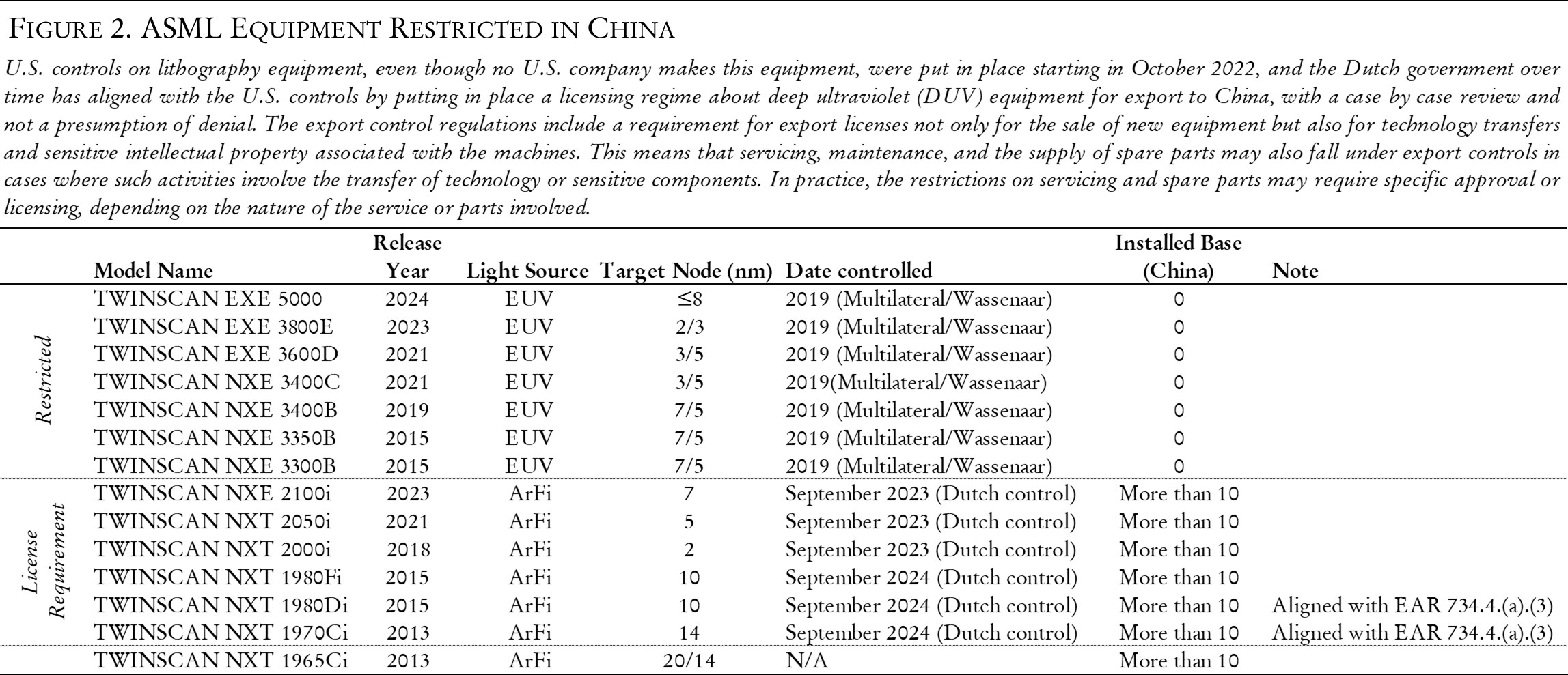
As I have noted previously, Chinese front-end manufacturers approach to the advanced lithography problem takes several paths. Manufacturers will continue to use advanced deep ultraviolet (DUV) tools from ASML for as long as servicing and spare parts allow. This has been further complicated by the new U.S. export controls in October 2023 and late 2024 restricting tool sales. It remains unclear how the Dutch government, working with ASML, will implement any new controls on ASML’s existing DUV installed base in China, particular at SMIC and associated facilities, including any involving Huawei affiliated personnel and R&D efforts. This raises many issues, such as overlay thresholds and how ASML handles software updates to its existing tools at now-restricted facilities in China, including SMIC’s.48
At the same time, it is increasingly clear that SMIC will not be able to get to something that can be called a 3 nanometer process using its existing DUV tools. Most industry observers agree that 5 nanometer is the limit here. SMIC’S so-called N+3 process could allow the firm to reach close to the density level of the TSMC N6 or Samsung 5 nanometer processes. In a best-case scenario, another iteration of process technology could mean achieving a node that is just marginally less capable than TSMC’s N5 process.49
Much has been written over the past year on Huawei’s efforts to pursue with SMIC and SiCarrier, techniques including quadruple patterning (SAQP)50 for using DUV down to 3-nanometer-class nodes.51 Huawei and SMIC have patented SAQP and other SAxP methods, as has SiCarrier.52 But industry experts are skeptical that it will be possible to use DUV based SAQP to get to 3-nanometer-class nodes. One well connected industry observer noted in November that “in discussions with a company that supplies materials to China’s semiconductor industry, he explained that doing SAQP the entire way is really difficult and SMIC still has not fully mastered this process.”53 Moving from some ability to do 7-nanometer-class node production down to 5-nanometer-class-node production is very difficult. Industry experts believe that getting to 3 nanometer-class node production via this pathway is not likely, and that efforts to move to EUV could prove successful before this could be accomplished.
Clearly Huawei, working with partners such as SMIC and SiCarrier, is doing R&D on methods for using existing DUV systems to get to more advanced nodes. But often the media reporting on this issue can be misleading, given how these companies push into areas that are beyond what other companies such as TSMC and Intel have done to try to extend the use of DUV systems to avoid using EUV systems. It is difficult to determine how successful these techniques will be and what the yields will be commercially.54 This approach does give Huawei and SMIC a path forward though, and substantial efforts are likely being expended to try and leverage existing patents and other industry expertise to this end. SiCarrier will be targeted in the latest round of U.S. export controls set to be released in mid-December. In late 2024, Huawei founder Ren Zhengfei admitted that the firm faced a challenging path: “American technologies and tools are very good . . . but Huawei cannot use them; we had no choice but to create our own tools. Open innovation and utilising the advanced achievements of others is the true way forward for an enterprise.” Ren’s comments suggest that Huawei intends to leverage a range of existing technologies and patents.55
The hope of getting to advanced lithography—capabilities resembling the extreme ultraviolet lithography (EUV) technique, which is the sole property of ASML—now appears to be firmly in the hands of Huawei. The Huawei-led effort is a long-term strategy that also includes other players. In September, for example, a 2023 patent related to EUV from domestic lithography leader SMEE was released, which revealed that SMEE has stepped up its R&D related to EUV. Huawei is likely leading and coordinating the overall effort.56 Huawei is also likely attempting to recruit engineers with expertise in key sub-fields critical to EUV from some of ASML’s suppliers.
Other major players focus on the other integral parts of an advanced lithography process. A significant MIIT release in September 2024 highlighted technologies, but not companies, involved in other critical process areas, such as wet cleaning, photoresists coating machines, ion implantation, and plasma etching.57 The table below identifies a few of the companies to which the MIIT release implicitly refers. Given the sensitivity of the topic of technical progress in all these areas, it would seem unlikely that the MIIT release includes any of the work being done under the aegis of Huawei at facilities all over China, and at advanced facilities featuring pilot production lines using domestic tools.
Beyond advanced lithography, China’s domestic toolmakers are all working on improvements to their tool offerings and attempting to balance the drive for self-sufficiency with maintaining ties to the global semiconductor industry. In August 2024, senior officials at leading Chinese toolmakers noted that the importance of etching, thin films, and other equipment grows as the role of advanced lithography changes.58

Taking Stock of China’s Domestic Semiconductor Industry
Just as the situation within the Chinese semiconductor industry in late 2024 was complex, so too is assessing where things go from here into 2025 and beyond. At the industry level, the situation is far more complicated than the performance of any single company would indicate, despite the attention on Huawei’s smartphone SoCs in the Kirin series. Within China’s technology sector, the focus has shifted well beyond achieving smaller dimensions on semiconductor nodes. Currently, there is a much broader debate regarding the systems engineering level, including chip design, device integration, and the use of new advanced memory sources. Beyond the semiconductor manufacturing sector, other, larger issues are at play. These include the need for a supporting development ecosystem as well as efforts to leverage new technologies such as silicon photonics, software-defined hardware, and advanced packaging methods. Perhaps even more important is the level of national policy, where Beijing has adopted new industrial supply chain organization and “national compute” strategies.
Seeing through the hype around new technology claims remains a challenge for observers. In October, for example, there was another story around a Chinese R&D breakthrough in silicon photonics, an important emerging technology, but likely not a game changer before 2030. This technology, however, is already being used for increasing transfer rates in data centers, and Huawei is exploring broader uses in those settings.59
Looking at both smartphone hardware and advanced GPUs can tell us something about the way forward. We can now compare the design of two different generations of smartphones based on the Kirin SoCs: the Mate 60 and the P70. The design of the Mate 60 smartphone, released in August 2023, included several systems engineering level improvements such as power supplies that have helped blunt some of the disadvantages of using process nodes at less advanced levels than other international market leaders. Compared to the Mate 60, the Pura 70 (P70) utilizes U.S. technologies to a far lesser extent. In some versions of the P70, estimates put the percentage of Chinese sourced parts at 90 percent.60 Though there is some controversy regarding the teardowns and how to estimate the total reliance on foreign sources of components, the trend suggests that engineers intend to design out 100 percent of non-Chinese components.
Designing out foreign components and technologies will remain a complex and evolving process. The core “system-on-chip” (SoC) has been marginally improved in the P70. But memory semiconductors may be the most important area of progress for Chinese domestic firms over the past two years and going forward. Industry reports suggest that YMTC provided the NAND flash memory in the P70, and it may have been packaged by Huawei.61 By contrast, the NAND memory in the earlier Mate 60 was likely made by a South Korean firm, SK Hynix, and drawn from stockpiles dating back to 2020–21.62 If this is true, it is a significant step forward for Huawei and YMTC, but Huawei still faces challenges obtaining advanced DRAM for its smartphones and other advanced consumer products.
Getting accurate information about progress at firms on the Entity List such as YMTC remains challenging, as these firms are not eager to publicize new breakthroughs. Some industry observers think that the LPDDR5 DRAM produced by CXMT will be good enough for Mate series smartphones for a time.63 Following YMTC’s December 2022 Entity List designation, the company launched a series of code-named projects, starting with “Wudang Mountain,” designed to iterate technological advances, remove U.S. toolmakers from production lines, and eventually, move entirely to domestic equipment.64 YMTC has been working particularly closely with a domestic firm, Naura, to replace U.S. toolmakers such as Lam Research and Applied Materials.65 Although the industry now finds itself in a highly dynamic situation, a number of trends can be identified for the next six to twelve months.
First, SMIC is likely working with Huawei and HiSilicon to attempt to improve yields at the 5–6 nanometer node and get production capacity to a level that will allow it to supply enough AI and server CPU semiconductors for Huawei and other top Chinese AI firms. This is almost certainly the near-term goal. In late September 2024, the South China Morning Post reported that Huawei has already supplied some major Chinese technology firms with samples of the Ascent 910C.66 Complicating this issue is the competing demand for Huawei Kunpeng server chips and Kirin SoCs, which almost certainly have a different yield than the Ascend series and are likely being produced on different process lines at SMIC and SMSC. Hence the challenge is keeping Huawei in a position to continue to produce a competitive phone SoC over a longer term, for say two to three years.
Swirling around any discussion of yields of advanced semiconductors at SMIC are the U.S. Commerce Department’s ongoing efforts to pressure U.S., Dutch, and Japanese toolmakers to limit support for their tools at SMIC’s most advanced production facilities. Last summer, problems with such tools likely slowed production of the Huawei 910B chip, according to some reports.67 This situation can fluctuate considerably depending on the availability of spare parts and the ability of technical staff to keep the tools running. While some reporting suggests only a 20 percent yield last summer for the Ascend 910B, it is likely that, as of October, this performance has improved to around 40 percent, doubling total capacity for Ascend series chips to roughly one million per year.68
Second, Huawei likely has its own backup strategy for the continual improvement of SoC and integral systems associated with the smartphone, server, and GPU application-specific integrated circuits. One crucial indicator will be the specifications on the new Kirin-9100 SoC: industry sources indicate that its CPU has not improved significantly, yet the Maleon GPU and power consumption have seen major improvements. Likely essential for progress will be access to some early generation HBM, which was not controlled for export to China as of October 2024. Prior to U.S. controls on HBM likely to be issued in mid-December 2024, Chinese firms including Huawei and Baidu were stockpiling HBM from Samsung.69 As the DRAM stockpiles Huawei has maintained since 2020–21 have been used in advanced smartphone designs while awaiting domestic alternatives, HBM stockpiles could be sufficient for domestic GPU makers like Huawei for some time. At present, however, it remains unclear where domestic sources of more advanced HBM will come from. Nonetheless, the iteration of designs and production processes within SMIC and Huawei, working with a variety of domestic and foreign toolmakers, is an irreplaceable engineering experience to develop capabilities that are impossible to gain any other way, helping all those involved climb the learning curve.
Many questions remain around the success of efforts to extend the capabilities of existing immersion DUV tools below the 5 nanometer node and a realistic timetable for Huawei and others’ efforts to develop advanced EUV-level lithography and associated supply chains. This timing will ultimately depend on which of the two most likely technological approaches succeeds.
The primary approach appears to use laser-produced plasma (LPP) for the light source. Industry observers believe that a prototype of this technology was already produced and is undergoing testing at an unknown location. This EUV project may see Huawei gain access to the light source and other components, after which it may begin work on the overall system next year, possibly in the major new R&D campus in Shanghai near to its design and manufacturing partners such as SMEE and SMIC.
Huawei’s likely goal is to roll out the capability in stages to facilitate the engineering learning process and ensure viability for high-volume manufacturing (HVM). The first stage would build on previous experience at the 5 nanometer node and aim to produce 5 nanometer semiconductors without relying on multi-patterning. If the elements of the system come together in 2026, then risk production could begin that year, and by 2027, we could expect to see HVM for commercial devices like Huawei’s smartphones in the Mate series. Some industry sources believe that this process is already far enough along that risk production before official approval could be done in 2025. All of these judgments should be considered with caution, given the difficulty in assessing from the outside how far along a host of different development paths are for choke point technologies.
A second, more experimental approach to EUV is steady-state microbunching (SSMB), as I noted in my previous article. At this point, central authorities appear to have only recently provided more resources to this completely different approach for the light sources. This suggests any system based on SSMB would not become viable until later this decade. While the LPP approach basically repeats the path ASML has taken, a new and unproven approach such as SSMB would also require additional breakthroughs in associated technologies, including masks, exposure imaging, reflectors, photoresists, and others.
Regardless of approach, Huawei’s efforts to obtain EUV will benefit from close collaboration with its partners in the industry. SMIC and Huawei, along with teams from major toolmakers like Naura, AMEC, and others, will likely have their top engineers working together at the new Huawei campus in Shanghai on a process that utilizes potentially both LPP and experimental lithography technology.70 Getting from a pilot line to HVM at sufficient yields, using an EUV system coupled with other tools and critical materials, will take at least one year. The potential gains from getting an EUV system up and running are so high in terms of throughput and yield, compared to techniques such as multi-patterning with immersion DUV, that they will likely spare no effort or expense in their attempt. Once a trial production line is fully operational, the whole effort would then be scaled up at a SMIC facility, likely one of the advanced fabs in Shanghai under SMSC.71
Looking Ahead to 2025
The challenges that leaders Huawei, YMTC, CXMT, SMIC, and the rest of the industry face in 2025 are considerable. The industry has progressed, however, beyond a point at which observers can simply compare technological capabilities using long-standing technical parameters. Critical technologies such as HBM and advanced packaging—coupled with developments in systems engineering, advanced AI-aided semiconductor design, and new ways to interconnect advanced chips such as GPUs—have redefined the industry’s benchmarks. Simple comparisons of raw computing power are less and less useful without accounting for such factors as the supporting software ecosystem, novel ways of connecting and powering tens of thousands of GPUs, and the changing designs of and training approaches for LLMs.
Observers need a different lens to measure where Chinese firms are relative to the global leading edge.72 That lens must include all four levels that I have attempted to define here: the semiconductor industry itself, systems engineering, the supporting ecosystem, and national policy.
Some experienced Chinese semiconductor industry officials have tried to deprioritize the efforts to achieve advanced node process capacity, calling it a risk whereby Chinese firms fall into a “path dependency” that becomes an obstacle to greater innovation. Industry veteran Ye Tianchun, president of the Integrated Circuit Branch of the CSIA, and vice president and secretary-general of the China Integrated Circuit Innovation Alliance, raised this issue in a nuanced speech at China’s twenty-sixth IC Manufacturing Annual Conference and Supply Chain Innovation Forum in Guangzhou in late May 2024. Ye noted that “external pressures [read U.S. export controls] will compel the Chinese IC industry to innovate its paths seven to eight years ahead of the global semiconductor industry.”73 Ye stated that such forward planning is necessary to avoid having Chinese firms focus primarily on catching up along a similar development path as the rest of the industry. Ye pointed specifically to the need for Chinese firms to improve the linkages between 3-D system packaging and product design architecture innovation. During his speech, Ye also observed that global logic device architecture is now shifting from FinFET to gate all around (GAA).74 Chinese firms will be challenged moving toward GAA architectures, as the United States finally imposed multilateral controls to restrict exports of GAA technology to China in August 2024.75 Ye is one of the top industry leaders who advise government agencies such as the NDRC on the status of China’s semiconductor industry and mapping China’s path towards and beyond current “choke point” technologies.
As the effects of the export control packages expand and reach more parts of the Chinese domestic semiconductor manufacturing supply chain, the need for Chinese companies such as SMIC, YMTC, and CXMT to make advances in manufacturing both logic (NAND) and memory (DRAM) chips faces significant challenges. At some point, stockpiling strategies exhaust their usefulness, necessitating a new approach or significant downgrades in performance of complicated finished systems such as smartphones and advanced GPUs and clusters. Access to HBM and other advanced memory will be a critical area for Chinese companies designing advanced systems in 2025.

U.S. export controls on memory remain controversial domestically. Most American industry players still claim that they find U.S. government justifications for including memory in the October 2022 restrictions package to be inadequate, given other controls on logic that limit progress at the cutting edge of performance.76 As of late 2024, domestic Chinese DRAM leader CXMT did not appear to be anywhere near capable of the R&D piloting needed to get to advanced HBM beyond HBM2E, without violating U.S. export controls.77 Whether CXMT can continue to avoid U.S. export controls while pursuing R&D in areas like advanced HBM remains unclear. Given that HBM is also a type of advanced packaging technique, other Chinese firms, including Huawei and packaging leader JCET, could also be involved in developing improvements for HBM.78 Lack of ongoing access to new generations of HBM will continue to limit the performance of the Ascend 900 processors.
Huawei will maintain a preeminent role within China’s semiconductor industry, despite some concerns about its dominance. As discussed above, Huawei’s leadership of semiconductor industry was one of the clearest and most notable developments within China’s technology sector in 2024. In October, the firm opened its Lianqiu Lake complex that has a floor area nearly 10 times larger than that of Alphabet’s headquarters in Mountain View, California.79 In addition, the Shanghai and Yangtze River Delta have become the epicenter of China’s semiconductor industry, with around 60 percent of the sector location there and now anchored by the new Huawei campus.80 Even so, as of late 2024, certain circles of China’s technology, academic, and research sectors have voiced concerns about the consequences of Huawei dominating so much of the sector. A leading computer scientist, Sun Ninghui, spoke out about Huawei’s dominance across multiple technology sectors.81 Another unnamed industry expert suggested that relying too much on one company would not support the development of a healthy innovation ecosystem, particularly as the Shenzhen conglomerate receives preferential treatment when competing for government procurement and in other ways. Others in the Chinese semiconductor industry thought these critics were making too much of Huawei’s role and that having a company such as Huawei be in a dominant position would help China overcome Western pressure via export controls and investment restrictions.82
In an October 2024 based on the technical teardown of a system that included Huawei Ascend 910B server semiconductors, TechInsights suggested that the 910B had been manufactured at TSMC, causing quite a reaction in the industry. It appeared that a third-party company, Sophgo Technologies, linked to a cryptocurrency billionaire, may have acted as a cutout to use TSMC foundry services to manufacture semiconductors on behalf of Huawei.83 Both companies deny this. The issue highlighted how U.S. export controls put TSMC in a very awkward position, where the firm is allowed to work with some Chinese companies but not others. The guidelines are murky and put the burden on TSMC to figure out complicated issues not part of the firm’s normal competence.84 While on the one hand working with Chinese smart device maker Xiaomi, which is not on the Commerce Entity List, makes it possible for TSMC to manufacture an SoC at the 3 nm node for a consumer handset, TSMC cannot do the same thing for Huawei, or on behalf of Huawei.
With GPUs, the situation is much more complicated. The changing performance thresholds in the October 2022 and October 2023 controls require a company like TSMC to determine how to determine whether the performance of a design exceeds the threshold before it even manufactures the product. Given the similarity in designs between crypto semiconductors, which do not fall under the performance thresholds in the Commerce rules, TSMC may not have been able to determine whether the design used in the 910B exceeded the GPU threshold or was being manufactured “on behalf of Huawei.” How TSMC could have known this is still unclear. Details of this story remain murky, and the author and other industry experts remain skeptical that Huawei could learn something from TSMC-manufactured semiconductors that would be useful for its collaboration with SMIC, as some have suggested.85 After all, Huawei was working very closely with TSMC prior to the FDPR rule that kicked in finally in September 2020.
In early November, in a significant development, TSMC appeared to have sent letters to clients in China indicating that will suspend production of AI semiconductors at the 7 nanometer node or smaller.86 This is likely to impact a much broader range of customers than previously covered by some of the performance-based restrictions, affecting Alibaba, Baidu, and other Chinese firms. The move was almost certainly a result of pressure from the U.S. Commerce Department and further pushes TSMC towards acting as an arm of U.S. export control policy. It also raises the geopolitical risks around the complex relationship between the United States, China, and Taiwan.87
At both the systems engineering and software levels, Huawei and its partners face considerable challenges; their actual proficiency is difficult for outside observers to judge. Achieving their goals for advanced semiconductor manufacture will depend on whether Huawei can pull together a consortium of companies that can make real progress toward commercial applications of a technology comparable to EUV lithography. Likewise, it is difficult to forecast when the software developers supporting advanced AI model training and other emerging applications will coalesce into an ecosystem on par with Western counterparts currently dominated by Nvidia.
Huawei has just recently cultivated an independent software ecosystem. In June, Huawei released the new version of the HarmonyOS operating system, which is not backward compatible with Android. Despite some five thousand companies reportedly agreeing to adopt the new HarmonyOS and fifteen hundred applications already in Huawei’s app store, some critics observed that major apps were not in the app store yet and many apps were designated as demo versions.88 Their criticism seems premature, given the major change that the new operating system represents; overall, it looks like HarmonyOS will be much more widely embraced by Chinese developers. The difficulty, however, will be to boost adoption of devices running HarmonyOS in foreign markets, where the firm’s previous offerings of smartphones using Android were very popular.
Developing a robust software support ecosystem, like that which it has for HarmonyOS, around advanced computing hardware such as GPUs will be a taller order for Huawei. As of the summer of 2024, major developers in China were increasingly moving development of AI models outside the Nvidia AI ecosystem.89 Chinese developers are used to working with foreign supporting software such as CUDA and Western AI development frameworks such as Pytorch and Tensorflow, for example. Getting the entire Chinese LLM development environment to switch to a putative Huawei hardware and software ecosystem will be challenging for both the firm and developers. Chinese companies and researchers are not as cut off from global AI development as one might expect, considering one explicit purpose of U.S. export controls. They still have access to increasingly capable open-source models from Western firms and still participate in international AI research conferences. Moreover, they have compute infrastructure personnel who are quite capable of designing advanced training systems using a variety of available hardware and software capabilities.
At the level of national policy, the context in which the entire rewiring of the semiconductor and supporting industry takes place, progress will accelerate in 2025 toward restructuring the sector around Huawei and around different types of government support, particularly bolstering R&D and building up “national compute.” As national-level data centers become more capable, they will be leveraged by smaller and medium-sized companies and potentially even larger players.
The ideological dimension of national policy will drive further change in 2025. A hint of the way forward can be gleaned from statements both from senior Chinese leaders such as Xi Jinping, but also from science and technology leaders in China. In July 2023, for example, the president of the CAS, Hou Jianguo eloquently stated the challenge that China faces, calling for the “acceleration of the seizure of a number of scientific and technological commanding heights in order to strongly protect national development and security.”90 Hou’s statement reveals how Chinese officials now believe that it is not sufficient for Chinese companies to catch up to their Western counterparts in strategic technological areas; rather, they must achieve some level of dominance to evade technological choke points in the future. This, of course, accords with the widespread view that Beijing desperately seeks to avoid the economic dependency and encirclement, which Chinese leaders see as fatal to their economic aims.
By the end of 2025, we should be in a better position to determine the near- and medium-term prospects for China’s semiconductor industry to close some of the technology gaps and overcome some of the identified technological choke points. Observers will also see whether the industry can utilize domestic innovations of a sufficiently broad and novel nature that would allow it to rival some Western systems of similar size and complexity. China’s semiconductor industry seems unlikely to “catch up” to the rest of the world, given the nature of the heavy controls imposed by the United States and allies as well as the complexity of the technology roadmap ahead. But, in 2023, no one in the U.S. government thought Huawei and SMIC would be able to produce a 7 nanometer SoC-based smartphone as they did with the Mate 60. Next year, Huawei and the Chinese semiconductor industry could once again astonish the world.
This article is an American Affairs online exclusive, published November 20, 2024. Figure 3 was added on December 6, 2024, after the announcement of a new round of U.S. export controls.
Notes
The author wishes to thank a number of industry observers who follow China’s semiconductor industry, both inside and outside of China. As noted above, because of the sensitivity around the topic, getting good information on the state of play of the industry in China requires significant triangulation, as there are few quality, unbiased sources readily available, particularly from sources that really understand the complex semiconductor supply chains. While I have tried to cite publicly available sources as much as possible, the nature of this topic requires that some authoritative sources, whose insights I have been able to verify, need to be left unidentified. [May need to edit based on inability to include most graphics: The author also wishes to thank technology policy researcher and DGA intern Ray Wang for his help on some of the graphics.] Having checked all sources for accuracy, the author also wishes to thank OpenAI and Anthropic for the use of ChatGPT-4o1 and Claude Sonnet 3.5 in aiding the conduct of research on this paper.
1 Kotaro Hosokawa, “China’s Chip Capabilities Just 3 Years Behind TSMC, Teardown Shows,” Nikkei Asia, August 31, 2024.
2 “Proposal on Respecting and Protecting Trade Secrets,” China Semiconductor industry Association, May 17, 2024.
3 Stu Woo, “China Is Getting Secretive About Its Supercomputers,” Wall Street Journal, July 23, 2024.
4 For more on China’s generative AI companies, see Paul Triolo and Kendra Schaefer, “China’s Generative AI Ecosystem in 2024 Rising Investment and Expectations,” National Bureau of Asian Research, June 27, 2024.
5 The “small yard and high fence” strategy is part of a broader approach to China and technology controls that I have dubbed the “Sullivan (China Tech) Doctrine.” It also highlights importance of advanced compute capabilities, including semiconductors, tools, and manufacturing capabilities, and AI as of high concern for the U.S. in terms of national security. For the “small yard and high fence” reference, see “Remarks by National Security Advisor Jake Sullivan on Renewing American Economic Leadership at the Brookings Institution,” The White House, April 27, 2023.
6 For a superb treatment of China’s export restriction, see Cory Combs, “Gaming out China’s Next Export Controls on Critical Minerals,” Trivium China, February 28, 2024; concerning tungsten, see Evelyn Cheng, “China’s New Rules Are Worrying Insiders About How Far Beijing Will Go on Controlling Critical Metals,” CNBC, August 22, 2024.
7 For example, see Wayne Williams, “Huawei Succeeds Where Microsoft Failed Miserably — HarmonyOS Now on Almost One Billion Devices, and China’s Largest Mobile Phone Manufacturer Has Completely Eliminated Android,” TechRadar, July 1, 2024; for more on China’s generative AI companies, see Paul Triolo and Kendra Schaefer, “China’s Generative AI Ecosystem in 2024 Rising Investment and Expectations,” National Bureau of Asian Research, June 27, 2024.
8 C.K. Tan and Kenji Kawase, “Wang Yi Says U.S. Sanctions on China Have Reached ‘Bewildering Absurdity,’” Nikkei Asia, March 7, 2024.
9 Phelim Kine, “Biden-Xi Phone Call Sparks Clash on U.S. High Tech Export Controls,” Politico, April 2, 2024.
10 Author discussions with senior administration officials, Spring 2024.
11 New rule to be issued in December 2024.
12 “Notice on Management Measures for Central Guidance Funds for Local S&T Development,” Ministry of Finance and Ministry of Science and Technology of the People’s Republic of China, December 28, 2023.
13 Regarding Ding, see William Zheng, “China Reveals Ding Xuexiang as Head of Communist Party Science and Technology Body,” South China Morning Post, June 27, 2024.
14 Author discussions with China based technology analysts, Summer 2024.
15 New rule to be issued in December 2024.; Bureau of Industry and Security, U.S. Department of Commerce, “Implementation of Additional Export Controls: Certain Advanced Computing and Semiconductor Manufacturing Items; Supercomputer and Semiconductor End Use; Entity List Modification,” Federal Register 87, no. 196 (October 13, 2022): 62186–215; “Public Information on Export Controls Imposed on Advanced Computing and Semiconductor Manufacturing Items to The People’s Republic of China (PRC) in 2020 and 2023,” Bureau of Industry and Security, November 6, 2023.
16 Bureau of Industry and Security, “End-Use and End-User Based Export Controls, Including U.S. Persons Activities Controls: Military and Intelligence End Uses and End Users,” Federal Register, July 29, 2024.
17 Author discussions with U.S. semiconductor companies, October 2022 – October 2024.
18 New rule to be issued in December 2024.
19 Author discussions with Japanese government officials, U.S. semiconductor companies, industry insiders, January 2024–October 2024.
20 For more on pushback from Japan and the Netherlands, see MacKenzie Hawkins et al., “ASML, Tokyo Electron Dodge New U.S. Chip Export Rules, For Now,” Bloomberg, July 31, 2024.
21 Discussions with industry insiders January 2023–October 2024. The authors note: Japan and the Netherlands, the two most important countries for chip-making equipment besides the U.S., have resisted additional controls out of concern they will hurt their own companies and damage relations with China.
22 On South Korean concerns about U.S. controls, see Sam Kim, “South Korea Wants U.S. ‘Carrots’ for Embracing China Chip Curbs,” Japan Times/Bloomberg, September 2, 2024.
23 For alleged threats of retaliation from Beijing, see Jenny Leonard et al.,
“China Promises Retaliation if Japan Expands Its Chip Export Controls, And Toyota Worries It’ll Get Caught In the Crossfire,” Fortune/Bloomberg, September 2, 2024.
24 Author discussions with government and industry officials, July–October 2024; media stories in late September hinted at a “Shadow Entity List”, see, for example, Ari Hawkins, “U.S., Japan, Netherlands Deals to Curb Chips to China Faces Delay,” PoliticoPro, September 30, 2024.
25 See, for example, Matteo Crosignani et al., “Geopolitical Risk and Decoupling: Evidence from U.S. Export Controls,” Federal Reserve Bank of New York, April 2024.
26 For more on this possible “death spiral,” see Paul Triolo, “Decoupling Without Direction,” Wire China, September 29, 2024.
27 Author discussions with leading U.S. semiconductor companies. Some supporters of the export controls, including a former Trump administration official in a September newsletter, point to the stock price of U.S. toolmakers in assessing whether these companies have suffered harm because of the controls. However, this argument is typically made those with little understanding of how the semiconductor industry innovates and how R&D budgets are determined. In fact, there is little correlation between the current stock price of a firm and that firm’s long-term performance, which is determined by its capacity to continue to fund R&D, which is contingent on its ability to maintain access to major markets and compete on a level playing field with competitors. U.S. unilateral export controls have created serious concerns about the ability of U.S. toolmakers to continue as global leaders.
28 Author discussions with Chinese industry observers in the U.S. and China.
29 Author discussions with industry observer, Shanghai, Spring 2024.
30 Amy Sarkar, “Huawei Set Up A Precision Manufacturing Company for 600 Million Yuan,” HC Newsroom (Huawei Central), December 28, 2021. The scope of business of Huawei Precision includes discrete semiconductor device manufacturing, along with non-descript offerings including engineering, technical research, experimental development, technical services, technical consultation, and technology transfer.
31 Author discussions with industry experts. The author’s own experience in 2019 touring the Mate 40 production line in Shenzhen suggested that Huawei’s internal capability to use its own equipment for critical parts of a complex manufacturing supply chain for consumer goods was already advanced.
32 Huawei holds a license for ARM’s latest Armv9 architecture, which was confirmed by ARM after a detailed review of its origins. Since the Armv9 technology is classified as UK-origin rather than U.S.-origin, it is not subject to U.S. export restrictions.
33 For example, see Raffaele Huang, “China’s AI Engineers Are Secretly Accessing Banned Nvidia Chips,”, Wall Street Journal, August 26, 2024.
34 For more on this, see Paul Triolo and Kendra Schaefer, “China’s Generative AI Ecosystem in 2024 Rising Investment and Expectations,” National Bureau of Asian Research, June 27, 2024.
35 Che Pan, “Huawei’s AI Chips Take Another Step Forward as Chinese Firms Look for Nvidia Alternatives,” South China Morning Post, 29 September 2024.
36 Che Pan, “China’s Nvidia Wannabe, Tencent-Backed AI Chip Start-Up Enflame, Flags IPO Intention,” South China Morning Post, August 28, 2024.
37 Fanny Potkin, “Chinese AI Chip Firms Downgrading Designs to Secure TSMC Production,” Reuters, June 4, 2024.
38 New rule to be issued in December 2024.
39 See Pei Li et al., “China Urges Local Companies to Stay Away From Nvidia’s Chips,” Bloomberg, September 27, 2024.
40 See, for example, Che Pan, “Chinese AI Chip Start-Up Biren Sees Performance Boost by Teaming With Tencent-Backed Firm,” South China Morning Post, November 6, 2024.
41 For an excellent treatment of this issue, see Katrin Bennhold and Ana Swanson, “The Battle to Control the World’s Most Powerful Technology,” The Daily, podcast audio, September 4, 2024.
42 The Biden administration has struggled to develop a strategy for monitoring and approving large-scale exports of AI servers for data centers around the world and particularly in the Middle East. In late September the U.S. Department of Commerce expanded its Validated End User (VEU) program to include some data centers outside the United States. This will almost certainly encompass G42 data centers in the UAE and elsewhere, in places such as Africa, that the conglomerate is building via a partnership with Microsoft. Commerce officials remain nonetheless concerned about large AI data centers in the Middle East potentially providing access to Chinese firms or diverting hardware to Chinese end users. It remains unclear how the U.S. Department of Commerce will monitor the VEU program as increasing numbers of AI data centers are built or planned around the world. For the VEU expansion, see “Commerce Updates Validated End User (VEU) Program for Eligible Data Centers to Bolster U.S. National Security, Promote Export Control Compliance,” Bureau of Industry and Security, September 30, 2024.
43 See Paul Triolo and Kendra Schaefer, “New U.S Chip Rules Could Be Very Bad, for American And Chinese Firms,” The China Project, October 5, 2022.
44 “China Beefs Up Computing Power as New Economic Catalyst,” State Council of the People’s Republic of China, July 7, 2024.
45 Ben Jiang, “China Telecom Say AI Model With 1 Trillion Parameters Trained With Chinese Chips,” South China Morning Post, September 30, 2024.
46 Training time can also vary depending on the ability of developers to leverage optimization strategies such as mixed precision training and data parallelism, something Nvidia’s deep AI development ecosystem supports. Huawei’s ability to assist developers using a China Telecom AI data center to train a one-trillion parameter model remains unclear.
47 Jian Yongxiang, “The World Is Shocked. Huawei’s New Machine Confirms the ‘Tashan Project’: The Schedule Is Faster Than Expected,” World Journal, October 16, 2023.
48 For an informed discussion of this issue, see Nicholas Welch, “Litho World & Commerce: Lost in Translation?,” China Talk, November 1, 2023.
49 Author discussions with industry experts, August–October 2024.
50 Self-aligned multiple patterning (SAxP), such as self-aligned quadruple patterning (SAQP), is an advanced lithography technique used in semiconductor manufacturing to achieve high-density, sub-10 nm features. SAxP involves using a series of deposition and etching steps to create multiple, precisely aligned layers that multiply the initial pattern density without solely depending on high-resolution lithography. Companies choose SAxP because it enables the production of smaller, more complex circuit features beyond the resolution limits of traditional lithography methods, improving device performance and power efficiency while extending the use of existing lithography tools.
51 See for example, Daniel Nenni, “Huawei Patent Reveals 3nm-class Process Technology Plans,” Semiwiki, May 29, 2024.
52 See, for example, Yijian Chen et al., Method of Metal Integration for Fabricating Integrated Device, World Intellectual Property Organization Patent WO 2023/236103 A1, filed June 8, 2022, and issued December 14, 2023.
53 Author discussions, November 2024.
54 See Daniel Nenni, “Huawei Patent Reveals 3nm-class Process Technology Plans.”
55 Iris Deng, “Huawei Founder Ren Zhengfei: US Tech Is Great, But We Have to Build Our Own,” South China Morning Post, October 31, 2024.
56 Che Pan, “Chinese Chip Making Shows Progress With New EUV Patent From Domestic Lithography Champion,” South China Morning Post, September 12, 2024; author discussions with industry observers, January 2024-October 2024.
57 “Notice of the Ministry of Industry and Information Technology on the Issuance of the “Guidance Catalog for the Promotion and Application of the First (Set) of Major Technical Equipment (2024 Edition),” Ministry of Industry and Information Technology of the People’s Republic of China, September 2, 2024.
58 “A Conversation Among Four Chinese Semiconductor Equipment Giants,” Geopolitechs, August 9, 2024.
59 See, for example, Xinmei Shen, “Chip War: China Claims Breakthrough In Silicon Photonics That Could Clear Technical Hurdle,” South China Morning Post, October 6, 2024. Silicon photonics is a technology that uses silicon as an optical medium to transmit, manipulate, and detect light for communication and computational purposes. It merges the fields of optics and semiconductor electronics, leveraging the advantages of both light-based communication and the scalability of silicon-based electronic manufacturing. Silicon photonics is increasingly used in data centers to enable faster and more energy-efficient data transmission between servers. Nvidia has explored using silicon photonics for its NVLink and NVSwitch architectures, which connect GPUs directly to enable massive amounts of data transfer with lower latency. With silicon photonics, these interconnects could potentially scale to even higher data rates, overcoming the bandwidth limitations of standard electrical interconnects.
60 Emiko Matsui, “Huawei Pura 70 Series Has 90 Percent of Chinese Components, Reveals New Report,” HC Newsroom (Huawei Central), April 29, 2024.
61 “Huawei Pura 70 Ultra — The NAND Within,” TechInsights, September 15, 2024. April 29, 2024; “YMTC’s Memory Developments Highlight China’s Strong Position,” TechInsights, accessed October 4, 2024.
62 “Huawei Mate 60 Pro — The Memory Within,” TechInsights, September 14, 2023.
63 Author discussions with industry insiders, October 2024.
64 See, for example, Atkinson, “Yangtze Memory’s Localized Production Line Has Made Progress, and Trial Production Will Be Launched as Soon as 2024,” TechNews, April 25, 2023.
65 Author discussions with industry insiders, March–September 2024.
66 Pan, “Huawei’s AI Chips Take Another Step Forward.”
67 Qianer Lu and Amir Efrati, “A New U.S. Crackdown Is Crippling China’s Best Hope to Rival Nvidia,” Information, June 25, 2024.
68 Author discussions with semiconductor industry observers, Fall 2024.
69 Heekyong Yang et al., “Chinese Firms Stockpile High-End Samsung Chips as They Await New U.S. Curbs, Say Source,” Reuters, August 6, 2024.
70 For an excellent examination of the Huawei campus and SMIC, see: Ana Swanson et al., “The Chinese Chipmaker at the Heart of the U.S.-China Tech War,” New York Times, September 16, 2024.
71 While I addressed some elements of the materials sector in China for semiconductors, tracking progress is complicated and will be the subject of a subsequent treatment. In May 2024, CSIA official Ye Tianchun in a conference speech, highlighted the fairly limited but significant progress Chinese firms had made in gaining domestic market share in key subsectors. Ye claimed, for example, that for 12-inch 28–45 nanometer process materials, domestic product types cover over seventy percent of needs; advanced process materials cover over seventy five percent. In developing photoresists, Ye claimed there has been breakthrough progress, with domestic i-line photoresist market share exceeding twenty percent; KrF photoresist market share reaching ten percent; ArF dry and immersion photoresists have begun small-scale application. Wet chemicals had achieved full supply for domestic fabs, with some products having an international market share exceeding forty percent. Advanced packaging materials such as die attach film, underfill, molding compounds, dielectric films, and CPU packaging thermal interface materials (TIM1) products have achieved small-scale supply from domestic sources. For more, see Zhang Guobin and Ye Tianchun, “Path Innovation, Change of Lanes of Development — Embarking on a Path of Integrated Circuit Innovation With Chinese Characteristics!,” EEtrend, May 23, 2024.
72 HBM can in fact be conceived as a kind of advanced packaging capability. HBM exemplifies advanced packaging technology by vertically stacking multiple DRAM dies and connecting them with through-silicon vias (TSVs). This 3D stacking is a characteristic feature of advanced packaging. HBM also integrates memory and logic in close proximity, often on the same package substrate. This aligns with the SiP concept, a hallmark of advanced packaging. Lastly, HBM often uses silicon interposers to connect the memory stack to the processor, which is another advanced packaging technique.
73 See Zhang and Ye, “Path Innovation, Change of Lanes of Development.”
74 Gate-All-Around (GAA) FinFET architecture is an advanced transistor design that enhances control over the channel region, improving performance and reducing power consumption compared to traditional FinFET structures.
75 Bureau of Industry and Security, “Commerce Control List Additions and Revisions; Implementation of Controls on Advanced Technologies Consistent With Controls Implemented by International Partners,” Federal Register, September 6, 2024.
76 Author discussions with U.S. semiconductor industry personnel, May–October 2024.
77 Amy Fan and Jay Liang, “CXMT Begins Mass Producing HBM2: China Aims to Reclaim AI Dominance?,” Digitimes Asia, August 2, 2024.
78 Author discussions with industry observers, July–October 2024.
79 Wency Chen, “Huawei Staff Arrive at New Mega-Campus, Hub of China’s tech Drive,” South China Morning Post, October 25, 2024.
80 IT Suro Fujino, “Huawei Courts Global Chip Talent with New Shanghai R&D Hub,” Nikkei Asia, November 5, 2024.
81 Dannie Peng, “‘Huawei Too Closed, Monopolistic’: Chinese Academic’s Rare Outburst Signals Emerging Rift,” South China Morning Post, September 26, 2024.
82 Peng, “‘Huawei Too Closed, Monopolistic.’”
83 Katrina Northrop and Eva Dou, “Export Controls Failed to Keep Cutting-Edge AI Chips from China’s Huawei,” Washington Post, November 1, 2024.
84 Some industry commentators have suggested that as a result of the still unclear situation with TSMC, Huawei, and Sophgo, that TSMC should devote more resources to compliance with U.S. export controls. TSMC already devotes significant resources to the issue, and it is not clear that the firm wants to be seen as an arm of the U.S. government in enforcing controversial elements of U.S. export control policy. In addition, this dynamic increases overall risks around Taiwan and China centered on semiconductors. For more on this, see: Paul Triolo, “The Taiwan Debate Is Heading in a Dangerous Direction,” The Wire China, July 14, 2024.
85 See Eliot Chen and Noah Berman, “TSMC’s Huawei Headache,” The Wire China, October 31, 2024. Given Huawei’s close working relationship with SMIC and other key players such as SiCarrier for techniques such as SAQP, which TSMC is not likely using for its 7 nm process, it appears high unlikely SMIC or Huawei would pursue a third-party arrangement with TSMC in order to learn about TSMC’s manufacturing processes.
86 Kathrin Hille and Ryan McCorrow, “TSMC to Close Door on Producing Advanced AI Chips for China from Monday,” Financial Times, November 8, 2024.
87 For more on this, see: Paul Triolo, “Sino-American Technology Competition and the Asia-Pacific,” in Asia-Pacific Regional Security Assessment 2022, International Institute for Strategic Studies, June 2022.
88 See, for example, Vivian Toh, “Huawei’s HarmonyOS Puts China’s Tech World in Awkward Spot,” Nikkei Asia, September 22, 2024.
89 Author discussions with Western observers of China’s AI development, July–October 2024. Some observers claim that there are large teams working on efforts to port elements of the CUDA architecture over to a system that will work with Huawei’s Ascend processors.
90 Hou Jianguo, “Strive to Seize the Commanding Heights of Science and Technology and Accelerate the Realization of High-Level Scientific and Technological Self-Reliance and Self-Improvement (In-Depth Study and Implementation of Xi Jinping Thought on Socialism With Chinese Characteristics for a New Era),” People’s Daily, July 17, 2023.
