In April 2024, eight months before his December “retirement” as U.S. semiconductor chip manufacturing champion Intel’s leader, its CEO Pat Gelsinger gave a remarkably frank public analysis of Intel’s ongoing difficulties.1 Once the global chip manufacturing leader, Intel at that moment ranked third among the only three remaining global companies mass producing advanced logic chips and made none of the most advanced chips, currently manufactured using 3 nanometer “technology node” fabrication processes.2 Intel’s most advanced chips in volume production internally were several generations behind the leader, Taiwan Semiconductor Manufacturing Corporation (TSMC), and lagged number two Samsung’s chips as well. Yet no other American company today even approaches Intel’s level of prowess in advanced, leading-edge manufacturing technology. Number two Samsung is credibly reported to be faltering as well, at the latest and most demanding 3 nanometer technology node, so is attempting to leapfrog to 2 nanometer chips. This currently leaves TSMC alone as the de facto leading-edge chip fabrication monopolist.3
The occasion for Gelsinger’s big reveal was Intel separating its public accounting and reporting into two separate, “virtual” companies, “Intel Foundry,” and “Intel Products.” Intel from its beginning had manufactured its own chip designs. Over time, the global chip industry had moved in a different direction: separation of the industry into specialized “fabless” chip design companies that do no manufacturing, and semiconductor “foundry” companies that only manufacture the designs of others. Gelsinger’s strategic analysis of Intel’s problems—resulting primarily from a radical change in the economics of the semiconductor chip manufacturing business—is fundamentally correct.4 This “radical” change in the economics of semiconductor fabrication, a change with consequences missed by Gelsinger’s most recent predecessors at Intel, left the company vulnerable as the pace of chip cost declines slowed during the first decade of the twenty-first century.5 Ironically, this big economic change was neither invisible nor particularly fast-moving, and its implications should have been grasped far sooner by Intel’s top management (and Intel’s board of directors), in the two decades preceding Mr. Gelsinger’s return to Intel in 2021.
Gelsinger was unable to fully execute a successful response to this economic shift during his truncated tenure as CEO, however, and to push his proposed new corporate “Intel IDM 2.0” business model. He resigned in 2024 under pressure from the company’s board.
Gelsinger’s strategy included continuing development of five improved sets of process technologies in four years and its next obvious stage: a formal Intel split into completely separate foundry and design (products) companies.6 Gelsinger had bet big—$100 billion in capital investments through 2027 in new production plants, serving the new foundry business model, at the expense of short-term profits—in order to restore Intel to a leading-edge position in chip manufacturing technology, with its currently emerging “18A” technology process. But his tenure ended before its 18A chips debuted. Intel’s foundry/design split accommodates very different business economic models, and from a U.S. defense policy perspective, very different national security imperatives.
Whether Gelsinger’s performance or the current Intel board’s impatience and shortsightedness bear ultimate responsibility for this implementation failure is unclear.7 Intel’s current problems were decades in the making. But this past history has now created an acute American defense industrial crisis with global national security ramifications. Before turning to the economics behind the current turmoil at Intel, we first consider the geopolitics of why Intel matters for U.S. national security.
National Security and the Rise of Semiconductors
Central to semiconductor technology development over time has been a series of focused interventions by governments, initially in the name of national defense, and more recently, national economic advantage. As we look at current developments in the semiconductor sector, we need to understand the major role played by the U.S. Department of Defense (DoD) in particular, in the evolution of the semiconductor industry.
The initial growth of the chip industry from the 1950s through the early 1970s was heavily dependent on a DoD willing to pay top dollar for bleeding-edge chip technology that would offset Soviet numerical advantages in weapons systems production, and technological advantages in rocket payload boost capabilities. Key elements of U.S. commercial chip manufacturing technologies were accelerated in the 1960s and early 1970s by both defense subsidies to R&D projects targeting improvements in performance and reliability of chips, as well as DoD willingness to pay breathtakingly high prices for chips meeting those goals.
DoD and NASA were almost the only customers for integrated circuit chips in their first four years of production.8 Integrated circuits (ICs) were the heart of defense computer systems, both for general purposes as well as specialized guidance systems for missiles and space systems. The Air Force largely paid for Texas Instruments’ (TI) first 1961 leading-edge IC factory (implementing the pathbreaking Fairchild Semiconductor silicon planar manufacturing process which cemented the reputation of Fairchild’s—later Intel’s—Robert Noyce as co-inventor of the IC with TI’s Jack Kilby).9 U.S. chip fabrication capability in metal oxide semiconductor (MOS) technology, which revolutionized chip design and manufacturing in the late 1960s and 1970s, was accelerated by funding by the National Security Agency (NSA) of exploratory projects at TI and a pair of pioneering startup MOS chip companies (AMI and GMe).10 Part of TI’s MOS group then left to form Mostek, which seized technological leadership from Intel and TI in computer memories in the 1970s and early 1980s. Fairchild also received substantial funding from the NSA to develop low power chips,11 but its slow commercialization of its internal MOS technology R&D was one of the frustrations prompting Noyce and Gordon Moore to leave Fairchild and form Intel in 1968, with production of cost-effective computer memory chips as a primary business objective.12
Even more importantly, the Central Intelligence Agency (CIA), Defense Advanced Research Projects Agency (darpa), and Air Force in the 1950s and 1960s had sponsored development of advanced optoelectronic technologies for use in spy satellites. With space and surveillance applications in mind, these same agencies supported a “micropower” research program intended to reduce feature sizes—and power consumption—on ICs by an order of magnitude. A prototype projection system from this project was created by DoD optical systems contractor Perkin-Elmer. Combining this idea with other technical advances developed for defense use in air and space optical surveillance platforms, Perkin-Elmer introduced a revolutionary new, commercially viable projection patterning system—the Micralign projection aligner—in 1973. It delivered hugely improved chip manufacturing productivity, and kickstarted a “great leap forward” in MOS chip manufacturing technology that continued from the mid-1970s until the present.13 Forty years of subsequent, steady, incremental improvements in chip patterning technology evolved into today’s schoolbus-sized Extreme Ultraviolet (EUV) lithography machines, selling for $250 to $400 million each, used in creating the densest and most energy-efficient chips powering recent artificial intelligence (AI) advances. (EUV is a media-friendly term describing what has also been called “soft X-rays.”14)
Today’s EUV monopolist, the Netherlands’ ASML, is built in large measure from the remnants of U.S. tech companies and their suppliers: Perkin-Elmer, whose chip lithography division was acquired by SVGL, in turn acquired by ASML with capital from Dutch Philips,15 and GCA, which shut down after failing to obtain needed capital from U.S. private and government investors in the 1990s. GCA’s advanced lens supplier, Carl Zeiss, became ASML’s lens producer.16 Japan’s Nikon, an earlier GCA lens supplier in the 1960s,17 ended up reverse engineering and improving GCA’s wafer patterning machines as part of Japan’s Very Large Scale Integrated (VLSI) Project, a government-industry cooperative R&D initiative of the late 1970s,18 accelerating GCA’s decline in the 1980s.) Perkin-Elmer’s Connecticut plant, now greatly expanded, remains as one of ASML’s two major U.S. plants.
In the mid-to-late 1970s, as commercial applications for this innovative chip technology exploded, and commercial markets surged well beyond DoD demand for leading edge chips, the direct DoD role in the U.S. chip industry’s success rapidly shrank. Defense Secretary Harold Brown and Undersecretary William Perry developed their “offset strategy” starting in 1977,19 using advanced electronics-based technologies and chips in defense systems, from cruise missiles to precision weapons to stealth to drones. Put most bluntly, defense access to leading-edge electronics, software, and computing capability, now mainly developed for use in commercial products, was expected by Brown and Perry to provide the U.S. military and its weapons systems with a technological advantage more than sufficient to offset the potential numerical superiority of possible adversaries in fielded manpower and weapons.
Early Challenges and the Rise of Fabless Chip Design
DoD’s offset policy met its first significant challenge in the early 1980s, when Japanese semiconductor producers surged ahead of U.S. manufacturers in the manufacturing technology used to fabricate the highest volume advanced semiconductors of the day, memory chips.20 Japan’s producers focused on improving semiconductor lithography patterning equipment (originally U.S. imports) for use in the largest “commodity” market for ICs: dynamic random access memory chips (DRAMs). They refined a production system for mass-market chips in highly automated ultraclean factories, obtaining higher yields and reliability at lower cost than U.S. producers. The ultraclean laminar air flow cleanroom technology used in these fabs was also initially developed in the U.S., at the Atomic Energy Commission’s Sandia Lab, and deployed by U.S. defense and space contractors in the 1960s,21 then introduced into Japan by TI Japan in the early 1970s.22 Refining these approaches, Japanese chip producers had become technology leaders in memory chip manufacturing by the early 1980s, benefitting from industry-wide tech initiatives organized by the Japanese government and NTT,23 then a state-owned telecom monopoly.
The Ronald Reagan administration responded with a multipronged national policy, negotiating “voluntary” restrictions on Japanese memory chip exports, applying significant pressure on Japan to buy more U.S. chips, and providing substantial funding for a successful partnership with the U.S. semiconductor industry on a cooperative R&D program to improve its chip manufacturing technology, sematech.24 The effort was largely successful, U.S. chip manufacturing regained its momentum, and the federal R&D subsidy ended in 1997.25
One unanticipated effect of the restrictions on Japan, however, was to assist entry by new producers in Korea and Taiwan into memory chip production. Most U.S. producers—like Intel—ultimately exited the commodity memory chip business and instead focused on manufacturing new kinds of chip designs, particularly microprocessors and other kinds of system and logic chip designs. The exceptions were TI and Micron Technology (founded by engineers from Mostek, the TI MOS technology spin-off which had become a memory chip tech leader in the 1970s), which moved production overseas to take advantage of state-funded financial incentives. TI eventually exited the memory market, opting to focus on design of signal processing and analog chips, and adopting a “fab lite” strategy that did not require huge investments in leading-edge chip factories.
Micron stayed in the memory business and focused on design innovation, cost efficient manufacturing overseas, and exploitation of scale economies. Micron also snapped up failed memory chip producer fabrication capacity at bargain-basement prices as the industry consolidated, including that of Qimonda (an offshoot of German electronics multinational Siemens) and TI,26 as well as that of Taiwanese and Japanese producers when they ultimately exited in the twenty-first century. Aside from recent and as yet unproven Chinese entrants, Korea’s Samsung and Hynix, and Micron, today are the only DRAM chip players left standing. (They were joined recently by new Chinese memory chipmakers selling primarily—at the moment—to the Chinese electronics industry.27) The same three companies plus Japan’s Kioxia (a Toshiba spin-off partnered with American firm Western Digital) are also the remaining (non-Chinese) fabricators of flash memory.
So-called “fabless” chip design houses that did no fabrication became increasingly important in the chip industry. Fabless firms include Qualcomm, Nvidia (which never owned fabs), IBM, and Advanced Micro Devices (AMD) after they divested their fabs to Global Foundries, and design groups within Apple, Google, Amazon, Microsoft, and Meta. The fabless design firms sent their designs off to be manufactured at so-called foundries in the United States, Singapore, Taiwan, and Korea, many of which only did manufacturing, and no design work on their own. The oldest, largest, and most important of these “pure play” foundry firms was in Taiwan—TSMC.
What became the foundry business started in the mid-1980s, benefiting from a substantial DoD investment from the late 1970s through the 1980s in chip design software tools, standards, and infrastructure. Defense-funded investments in chip design technology and standards in that period supported U.S. leadership in chip design, and this underlay the explosion in fabless chip design in 1980s and 1990s, as well as the creation of the foundry business model developed by TSMC after 1987. Most notable was work in the late 1970s by researchers at Caltech and Xerox PARC to develop a greatly improved system for VLSI (Very Large Scale Integration) chip design using advanced software tools.28 Further development of these tools enabled the complete separation of chip design from chip manufacturing, and the development of fabless (design-only) and foundry (manufacturing-only) chip firms which followed. This work was picked up and supported by darpa in 1978, and became the foundation for its VLSI program, which approached $100 million in annual funding by 1982.29 By the mid‑1980s, the initial darpa program had been subsumed into an even larger, early darpa effort to create a U.S. industrial base for artificial intelligence applications: the Strategic Computing Initiative.30 Though unsuccessful in creating fully autonomous military weapons platforms, this effort underwrote important advances in parallel computing architectures, expert systems, and information-aware battlefield command and control systems.31
After 1997, the cooperative industry-government effort to improve chip manufacturing technology housed at sematech was continued by industry for more than an additional decade, with little federal funding, and a new focus on coordinating emerging standards and technology required for successive new generations of manufacturing technology and required equipment and materials. The effort brought together developers of the specialized bits of technology, created by an increasingly globally dispersed and fragmented set of supplier firms with their customers, to launch new semiconductor technology “nodes” (indexed by the minimum feature sizes of the chips they could create—like 130 nanometers, 90 nanometers, etc.) on a predictable schedule. The sematech-led coordination effort (known as the International Technology Roadmap for Semiconductors—the ITRS) was successful, with new generations of manufacturing technology being introduced every two years into the second decade of the twenty-first century.
Sematech and the ITRS effort fell apart after 2010, fundamentally because the scale of investments required to stay at leading edge in chip fabrication had led to a sharp decline in numbers of chip-making firms investing in the manufacture of the most advanced chips. There was simply no economic incentive for the few surviving leading-edge chip producers to coordinate with lagging manufacturers lacking the scale to invest in leading-edge manufacturing.
Federal Interventions after the Cold War
With the end of the Cold War in the early 1990s, the pressure for maintaining a U.S. semiconductor technological advantage largely diminished. This was not to last.
To be clear, episodically, national security interests motivated provision of critical government assistance to private sector efforts despite the end of the Cold War. One good example is EUV silicon wafer patterning technology. Intel, along other chip producers and semiconductor equipment and materials companies, formed a consortium operating at the Department of Energy’s Lawrence Livermore National Lab in 1997 to develop EUV patterning technology.32 The complex, laser-produced light source used in current EUV patterning equipment utilizes laser technology developed for creating fusion reactions within that lab.33 In general, however, the national security role in providing resources and markets to drive semiconductor manufacturing technology forward was much diminished with the Cold War’s end, and DoD in the early twenty-first century mainly struggled to keep abreast of commercial semiconductor technology for most kinds of digital logic and memory chips.
But DoD microelectronics efforts did not end with sematech. Semiconductor R&D continued at a modest level at darpa over following decades. Prior to the chips Act legislation, and in many ways anticipating it, darpa in 2017 began an Electronics Resurgence Initiative (ERI) to develop new semiconductor materials, designs and architectures;34 this was renewed in 2023 as ERI 2.0 to promote U.S. technology leadership in next generation microelectronics research, development and manufacturing.35 Darpa later received additional funding in the chips Act for this program.
Three decades past the end of the Cold War, however, global military competition is resurgent, and chips are once again increasingly central to national security. This development is not visible in DoD’s share of the overall semiconductor market, which is less than 1 percent. The great bulk of its current needs for existing weapon-system platforms are in so-called legacy chips: 11 percent of its chip spending is for chips under 28 nanometers, 18 percent for chips between 28 and 90 nanometers, and 66 percent for chips between 90 and 350 nanometers.36 The existing DoD inventory of weapons and systems largely does not require the most advanced chips used in commercial equipment (though DoD does require the most advanced signal processing and analog chips, typically supplied by specialized U.S. producers catering to national security requirements).
But it is increasingly clear that the emerging technologies that will decide future conflicts will once again require the most advanced digital logic and memory chips. Artificial intelligence, quantum computing, advanced data centers, and autonomous drones, for example, are now realities, and will require ever faster, ever more powerful and ever less power-hungry chips, and nations with early and assured access to such chips will be able to seize technology dominance.
“Moore’s Law,” announced in 1965 by Intel cofounder Gordon Moore, came to stand for the presumption that every two years chips would double in capability and prices would fall by half.37 While the chip industry over the last decade has clearly fallen off the Moore’s Law pace, with costs for advanced chips no longer falling rapidly and capability increasing more slowly, the chip demands of potentially game‑changing technologies like AI and quantum computing now require DoD to be the first to field equipment making use of advanced chips needed in these applications. National security now requires DoD to regain its position as the premier military user of leading-edge chip technology.
The Present Crisis
That is how we now find ourselves in a moment of national security crisis. Taiwan, which now produces 100 percent of the most advanced chips used in U.S.-designed systems, is eighty miles offshore from a more and more militarily assertive China. China views Taiwan as a breakaway province, has long announced its plans to reassert control, as recently reiterated in Xi Jinping’s 2025 New Year’s greeting,38 and has been increasing the pace of invasion training exercises. With China’s continuing military buildup, the willingness and ability of Taiwan, and the U.S. Seventh Fleet, to block an invasion or prevent a blockade has appropriately come into question. China’s navy is now larger than the U.S. Navy, with 395 ships compared to 296. China is also building vessels at a considerably faster pace than the U.S. Navy, which must maintain a multi-ocean presence.39
Until its new U.S. fabrication facility is completed, TSMC’s more advanced chip fabs have been entirely located in Taiwan. Korea has only a slightly better strategic location, close to China and even closer to an unpredictable and fanatical North Korean regime supported by both China and Russia.
The potentially dire national security situation was aggravated in December 2024 by public remarks from Morris Chang, TSMC’s celebrated founder, generally disparaging Gelsinger and Intel after the CEO’s exit.40 Previously, in October 2021, Chang had publicly criticized Gelsinger as “cocky” and “discourteous.”41 This was after Gelsinger reportedly offended TSMC by publicly saying “You don’t want all of your eggs in the basket of a Taiwan fab” in May 2021. This followed another December 2021 utterance, according to a media source, in the course of “encouraging U.S. investment in U.S. chipmakers, [Gelsinger] said at a tech conference: ‘Taiwan is not a stable place.’”42 These less than diplomatic remarks were reported by Reuters’ multiple Taiwanese sources to have led TSMC to cancel a 40 percent discount it was giving Intel on prices for fabricating Intel chip designs on TSMC wafers.43
This discount, or lack thereof, was a serious and possibly critical business issue for Intel. The slides accompanying Gelsinger’s frank April 2024 webinar,44 mentioned at the outset of this article, show an Intel reliant on external suppliers—e.g., TSMC—for about 30 percent of its fabricated wafers, which, sliced into individual Intel-branded chips, or chiplets combined with less advanced Intel silicon, are packaged and sold as Intel chips in global markets. Put another way, about 30 percent of chip sales by Intel Product (the new Intel division that designs Intel chips), by volume of silicon (and most likely a higher percentage of revenues), are produced by what are effectively fabless Intel chip design groups. These designs are fabricated outside the company, i.e., manufactured outside of the current Intel Foundry (whose not-so-advanced technology nodes currently suffer from excess capacity, per the April slides). Included in the 30 percent of Intel wafers ordered from TSMC by fabless Intel chip design groups are most, if not all, of its most advanced and complex chip designs, like its Gaudi AI accelerators, its Alchemist and Battlemage graphics processors, and its most recently minted AI-enabled Lunar Lake x86 architecture processors.
If the Reuters reporting is correct,45 TSMC’s cancellation of such a large discount could have contributed to Intel’s faltering financials and Gelsinger’s December demise. Whether or not this retaliatory action was executed by TSMC, an important lesson should be learned. If TSMC’s emerging leading-edge chip fabrication monopoly (given the setbacks faced by Intel and now Samsung) threatens to raise its prices, or even to cut Intel off entirely from cutting-edge chip supplies, Intel has no alternatives other than to simply beg for supplies. That is the implication of TSMC’s developing monopoly on the most advanced chips. TSMC’s Taiwan development and production fabs are currently the only foundries capable of fabricating what are now Intel’s most advanced and complex chip designs. Worse, Intel’s vulnerability shows the potential vulnerability of all U.S. chip design groups producing advanced logic and system chips, at Nvidia, Qualcomm, AMD, Amazon, Apple, Google, Meta, Microsoft.
For any defense contractor or government user with an imperative current or future need to access the most advanced available chip manufacturing technology, reliance on a sole Taiwanese source is a significant national security risk. This reality requires open dialog with Taiwanese colleagues, not hiding growing concerns away from view.
Taking a narrow view, the short-term national security threat may look less severe than the economic risk. Few of these most advanced, Taiwan-only fabbed chips are currently designed into fielded weapons platforms. By contrast, the most advanced fielded IT products and services currently being sold by cutting-edge U.S. information tech companies are, or will be, entirely dependent on TSMC chips fabbed in Taiwan.
But over the long term, the national security risk is even graver than the economic threat: because of the rapid recent development of AI capabilities and a pressing need to incorporate powerful new information technology making use of AI into U.S. defense systems, and because none of the next generation of most advanced leading-edge fabrication capacity will be physically located in the United States, where production priorities in times of dire U.S. national emergency are potentially subject to Defense Production Act (DPA) authorities.
Gelsinger’s language may have been undiplomatic, but, unfortunately, it accurately describes a supply chain risk that America in the last few years has been taking very seriously. TSMC’s Chang, on the other hand, ignores legitimate U.S. national security interests when he suggests that Intel should abandon its foundry business (which will compete with TSMC’s) and focus on designing successful AI chips (locking it into a pure TSMC customer role).
The fact is that the United States has no fundamental national security interest in assuring the survival of Intel Products—Intel’s chip design business—which aspires to compete against the many other U.S.-based companies designing and selling both AI-related chips and AI services making use of these chips, as well as computer processors (CPUs), graphic processor units (GPUs) and customized accelerator chips used for AI, networking, and other logic and systems chips. In contrast, the United States has an overwhelming national security interest in ensuring that DoD and its contractors have access to a U.S.-located foundry that can develop and use cutting-edge manufacturing technology to produce advanced AI accelerator chip designs, and other advanced chips now and into the future. Making Intel Foundry a success is the only current option that assures U.S. access to a U.S.-located leading-edge chip manufacturing technology development and production capability should supply chains in East Asia be obstructed by military action.
This situation could change if U.S.-Taiwan security discussions were to frankly and explicitly address the vulnerability of global supply chains running through Taiwan to military pressure from China. To guarantee that Taiwan’s own military forces can replenish their armaments in the face of military pressure from China, as a quid-pro-quo for U.S. commitments to assist Taiwan with its defense, Taiwan should be willing to take steps to assure U.S. access to the most advanced chip manufacturing technology developed at TSMC, under scenarios that reduce or interrupt output from TSMC’s Taiwan fabs. To be counted as a reliable sole source for critical components needed by the U.S. defense industrial base, TSMC should be willing to both develop the next generation of leading-edge technology, and manufacture using the current generation of advanced chip manufacturing technology, within high volume North American facilities, in parallel with any Taiwan-located development and production facilities.
In other words, the only circumstance under which TSMC, the leading-edge monopoly chip company, can truly de-risk its status as a sole source supplier to U.S. chip design groups is if TSMC has U.S.-located development and production capacity that mirrors leading edge capabilities now only present in Taiwan. Nevertheless, this commitment likely will require further U.S. subsidy as well as changes to Taiwanese laws to make it an economically viable proposition. In addition, TSMC’s rich talent base and huge chip production infrastructure lock it into its Taiwan location for a long time to come, even if it is now building essentially two follow-on plants in the United States which will produce at levels lagging well behind TSMC’s fabs in Taiwan. These are significant barriers to meeting U.S. security needs. Nonetheless, a realistic security dialogue with Taiwan and TSMC should commence. But a successful and healthy leading-edge Intel Foundry realistically remains the only current policy option that deserves U.S. public subsidy on both national security and economic security (supply-chain risk) grounds.
The CHIPS Act and National Security
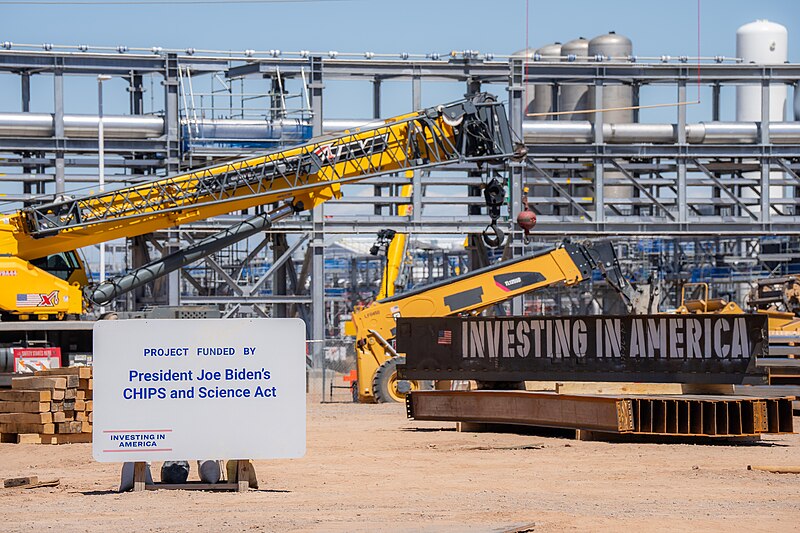
In 2022, motivated by these glaring national security considerations, Congress passed and funded, with bipartisan support, the chips Act, providing $39 billion in grants, $75 billion in loan guarantees, and $24 billion in tax incentives for new semiconductor fab construction in the United States, plus $11 billion for semiconductor R&D.46 The funding has helped leverage private sector investment in a series of new fabs being built in the United States, including four by Intel in Arizona and Ohio, two by TSMC in Phoenix, and two by Samsung in Texas. Overall, the federal commitment has helped leverage an estimated $834 billion in private sector investment in U.S.-located fabs,47 although these numbers have slipped slightly in recent months because of a post-Covid decline in computer central processing unit (CPU) demand.48 Chips Act–driven investments may nudge the share of world chip output produced in the United States up from 12 to 15 to 20 percent.49
The chips Act obviously marks a dramatic change in the U.S. government’s attitude to semiconductor plant financing—it is a clear defense industrial policy. It is important to keep it in perspective, however: China has $142 billion in government financing either underway or planned and has more fabs under construction than any other nation.50 Europe has its own chips effort with $46 billion, and Korea, Japan, and Taiwan are all making major investments.
This brings us back to the geopolitics surrounding Intel. Both TSMC and Samsung retain the great majority of their advanced chipmaking in their own home countries and will continue to do so. In fact, Taiwan has established regulations preventing next generation chips from TSMC from being produced outside of Taiwan, in an effort to assure that advanced chip production leadership stays in Taiwan (and perhaps, creating a “tech hostage” that the United States will be compelled to defend).51 Four new fabs in the United States from TSMC and Samsung may help through 2030 in assuring DoD access to recent-generation advanced chips, but will not provide access to the next round of the most advanced chips. These new fabs do not fully solve the U.S. national security problem, and do not solve potential supply chain security problems in an era when economic or supply-chain security is a vital component of national security. With “chips in everything,” if TSMC production collapsed after an invasion, the effect on the U.S. economy would be prompt and dramatic.
Over the longer term, the threat to U.S. national security from a Chinese takeover of Taiwan would be even more profound, arising from two factors that are rarely discussed when this issue is considered. First, while close to half of human chip designers are physically located in the United States, about 20 percent are located in Taiwan (historically facilitated by convenient local availability of foundry capacity). Though the U.S. share of chip design revenue and its ability to train designers to meet demand have slipped in recent years, chip design capability remains a crown jewel in the U.S. technology industrial base.52 As we emphasize below, from a security perspective, those Taiwanese chip designers are a human resource as or perhaps even more important than the physical fab capacity in Taiwan that is producing the world’s most advanced chips.
Second, TSMC, in Taiwan, possesses, or is able to access, forty years of chip design information for the many chip designs, or “tapeouts,”53 supplied to it by its many customers throughout the world. In a doomsday, worst case scenario, if TSMC’s tangible and intangible assets were to become subject to China’s 2017 National Intelligence Law,54 then the Chinese government could compel access to those decades of tapeouts as critical to China’s national security. The tapeout for a chip, combined with relevant information in the TSMC Process Development Kit (PDK) for that chip, could be used to first reverse engineer a mapping of transistors and their connections as implemented in the chip (a “netlist”), and combining that, in turn, with some expert engineering knowledge, the logical and functional design of a chip could ultimately be deciphered.
If, as we believe to be the case, current generation AI technology has already demonstrated that chip design tools can be trained with more and better chip design information to further automate the costly process of chip design, then the decades of chip design tapeouts in TSMC’s cyberspace vaults are an extremely valuable database that could ultimately be used to engineer leaps forward in application of AI models to chip design. Rapid and inexpensive AI-assisted chip design has the potential to both greatly reduce cost and accelerate the insertion of leading-edge chip designs into both military and commercial applications. Access to the accumulated inventory of chip tapeouts used in the manufacture of chips by TSMC, by far the largest foundry in the world, past and present, could prove as or more valuable than the physical TSMC fabs located in Taiwan.
As the only U.S. firm in a practical position to build leading-edge chip production capability in the U.S. within a realistic time horizon, Intel is no longer just another U.S. private sector company; given the geopolitics, it’s a different animal.55 The United States, as a matter of national security, has a significant stake in the survival and success of the leading edge “Intel Foundry” entity that Intel has created. Given its massive fab infrastructure and R&D capability, it is not replicable in any reasonable timeframe by another U.S. firm; its former American chip competitors have long since pulled out of the advanced chip manufacturing competition.
This brings us to the changing economics of producing leading-edge chips, why we think Gelsinger’s strategic analysis is fundamentally correct, and what the U.S. should be doing to maximize not just Intel’s, but all U.S. semiconductor companies’ technological lead within a rapidly changing global economy. We will address these issues in detail in a future article. Clear-eyed analysis of the path forward for America’s struggling national champion, Intel, is required, along with a broader approach to rebuilding the U.S. semiconductor manufacturing sector. It is important to recognize that the chips Act is a stopgap measure. It assures some production in the United States of the pending generation of advanced chip processes,56 but not the following generations of chips. It was a onetime law; the authorization runs out in 2027, and the funding for constructing new fabs is already committed. The U.S. semiconductor challenge is a long-term one and this was an important but decidedly short-term fix.
Continued financing is not the only need. Major longer-term initiatives backed by DoD are needed in areas such as leveraging AI to radically reduce the cost of advanced semiconductor designs, and for post-CMOS R&D—both offer technology leap-ahead opportunities of first-rank importance. DoD also needs to integrate its current R&D and design efforts with programs evolving at the Commerce Department into a single, coherent national initiative.
Recapturing a leadership role in advanced chips will not be easy or cheap. But the national security implications of failing to do so are profound and disturbing. The defense-industrial crisis that must be addressed is upon us.
This article originally appeared in American Affairs Volume IX, Number 1 (Spring 2025): 40–54.
Notes
1 Intel,
“New Segment Reporting Webinar,” Intel Newsroom, April 2, 2024; CNBC staff, “
Intel CEO Pat Gelsinger: We Expect the Foundry Business to Break Even in 2027,” CNBC, April 5, 2024.
2 The “technology node” in nanometers nomenclature originally was a well-defined descriptive term—the size of the smallest length feature that could be reliably patterned on a chip. For advanced technology nodes after 20 nanometers (i.e., indexed by a number below 20 nanometers, after fully three-dimensional transistor structures had been adopted by all advanced chip fabricators), however, actual minimum two-dimensional feature sizes are generally greater than indicated by the nanometer index number, and process technology node number is best regarded as an ordinal index, ranking minimum feature size relative to other processes previously used by that same manufacturer. They also are no longer comparable across manufacturers—for example, Intel’s 10 nanometer process was said to be comparable in transistor size to TSMC’s 7 nanometer process and Global Foundries’ 12 nanometer process. Intel now uses advanced technology node descriptions referencing angstroms (A) rather than nanometers (10 angstrom = 1 nanometers). Intel’s current 18A technology node is denser (more transistors per unit area) than TMSC’s competing 2 nanometer process, but these are both categorized as “2 nanometer” class fabrication processes. Since the demise of the International Technology Roadmap for Semiconductors (ITRS), circa 2014, these process technology node description numbers no longer have a well-defined, standardized dimensional attribute associated with them that is comparable across manufacturers and over time.
3 See, for example: Woo Ji-Han and Lee Jae-eun, “Samsung Sets Sights on Foundry Revival With 2nm Turnaround,” MSN, December 2024; Mihal Matel, “Low 3nm Chip Yield Might Spell Trouble for Samsung’s Exynos 2500,” Sammobile, November 6, 2024; Neil Jerome Morales and Heekyong Yang, “Samsung Says It is Not Interested in Spinning Off Foundry Business,” Reuters, October 7, 2024; Mihal Matel, “Samsung Might Be Having Major Issues at Texas Chip Plant,” Sammobile.com, September 16, 2024; Charlotte Trueman, “Samsung Issues Apology ahead of Q3 Results,” Data Centered Dynamics, October 8, 2024; Majeed Ahmed, “The 2-nm Process Node and Samsung’s Foundry Crossroads,” EDN.com, December 18, 2024; Jean Leon, “Samsung Discloses its Plan to ‘Defeat’ TSMC and Keep SMIC At Bay,” Android Headlines, December 10, 2024; Abdullah Asim, “Samsung Foundry Disbands Development Division, Possibly Giving Up on 2 Nm Production,” Phone Arena, December 5, 2024.
4 After his December 2024 forced departure, interest in a YouTube video of Gelsinger from 2023 in which he insightfully articulated three Intel “big misses” surged. The three misses were: the mobile phone wave, fumbles in AI, and internal Intel “anti-foundry” bias. All three of these big misses are directly connected to the structural economic change. See: Digit, “Pat Gelsinger Talks about Intel’s ‘Big Misses’,” YouTube, October 6, 2023, 0:58. These “misses” are discussed in our future article.
5 In technologically more precise terms, the pace of what semiconductor technologists called “Dennard scaling” slowed dramatically. See: Kenneth Flamm, “Measuring Moore’s Law: Evidence from Price, Cost, and Quality Indexes,” in Measuring and Accounting for Innovation on the 21st Century, eds. Carol Corrado, Jonathan Haskel, Javier Miranda, and Daniel Sichel (Chicago: NBER & University of Chicago Press, 2021), 406–13.
6 Intel, “Intel CEO Pat Gelsinger Announces ‘IDM 2.0’ Strategy for Manufacturing Innovation and Product Leadership,” Intel Newsroom, March 23, 2021; Intel, “Pat Gelsinger on Foundry Momentum, Progress on Plan,” Intel Newsroom, September 16, 2024.
7 Dylan Patel et al., “Intel on the Brink of Death,” Semianalysis, December 9, 2024; Doug O’Laughlin, “The Death of Intel: When Boards Fail,” Fabricated Knowledge, December 3, 2024.
8 DoD and NASA bought 100 percent of integrated circuit production in 1961 and 1962, 85 percent in 1963 and 1964, and 72 percent in 1965. See: Charles Fishman, “How NASA Gave Birth to Modern Computing,” Fast Company, June 13, 2019.
9 Rosemary Remancle, “Oral History of Charles Phipps,” Computer History Museum, May 28, 2009, 19.
10 MOS startup pioneers AMI and GMe, a Fairchild Semiconductor spin-off, were supported by these NSA projects. NSA interest reportedly was stimulated by the higher density possible (“200–300 circuits per die”) with the new technology: “you could get enough circuits on one die to do a basic part of a key generator in their crypto work, and you didn’t have to expose it on a [printed circuit] board. It meant quite a bit to them security-wise to have it all [encapsulated] in one package, and you could—they went so far as to put explosive powder under the lid so if it were tampered with, it would blow away the metal and you couldn’t see what was done.” See: Remancle, “Oral History,” 21–22.
11 Fairchild’s second generation Milliwatt Micrologic ICs became known internally as the “R13” circuits, after the NSA group (R-13) that sponsored their development: “that’s how we got the [NSA] R-13 contract, which was a second generation of DCTL integrated circuits, designed for lower power and with higher complexity devices. And at that time, of course, it was all communications, security stuff.” See: David Laws, “Oral History of Panel on the Development and Promotion of Fairchild Micrologic Integrated Circuits,” Computer History Museum, October 6, 2007, 29–30; David Laws, “Oral History of Robert (Bob) H. Norman,” Computer History Museum, May 7, 2009, 21; David Laws, “Oral History of James (Phil) Ferguson,” Computer History Museum, April 29, 2010, 14–15; Bill Welling, “Fairchild Oral History Panel: Bipolar Digital Products,” Computer History Museum, October 5, 2007, 10–11.
12 MOS transistor technology initially sacrificed switching speed in order to achieve higher density (more transistors per silicon area) and lower power requirements. High performance computing, the major developing market for commercial use of integrated circuits in the 1960s, was focused primarily on performance, and therefore, speed.
13 Christopher Mason, “50th Anniversary of Micralign: A Retrospective,” SPIE Digital Library, April 30 2023; “Interview with Phil Pressel, formerly of Perkin Elmer,” National Museum of the US Air Force, Hexagon KH-9 Reconnaissance Satellite, 2015.
14 This terminology change reflected engineer concerns about their management supporting “X-ray” chipmaking projects. Email communication from Dan Hutcheson, January 8, 2025.
15 Craig Addison, “Losing Lithography: How the US Invented Then Lost a Critical Chipmaking Technology Process,” SemiWiki, Oct. 31, 2021. See also: Oliver Hamrin, “The Silicon Empire: TSMC’s Revolution and Morris Chang’s Legacy,” Quartr, August 27, 2024.
16 GCA later purchased another lens supplier, Tropel, which was ultimately acquired by Corning after GCA shut down. Tropel went on to manufacture optics used in development of ASML’s EUV technology by the National Labs’ EUV consortium. See: Anthony Yen, “EUV Lithography for the Age of AI,” IEDM, October 31, 2024, 16.
17 Nikon had previously supplied lenses used in GCA mask-making equipment. “1960’s Photo Repeater,” Semiconductor History Museum of Japan, May 11, 2022.
18 See: Kenneth Flamm, Mismanaged Trade: Strategic Policy and the Semiconductor Industry (Washington, DC: Brookings Institution, 1996), 110–11.
19 Edward Keefer, Harold Brown: Offsetting the Military Challenge, 1977–1981 (Washington, DC: Historical Office, Office of the Secretary of Defense, 2021), 575–601.
20 Hideki Tomoshige, “Japan’s Semiconductor Industrial Policy From the 1970s to Today,” CSIS, September 19, 2022.
21 Philip Naughton, “History of Cleanrooms,” Ashre Journal, November 2019, 46–50.
22 Sandia Laboratory engineer Gordon King left its cleanroom group in 1965 to join TI, where he designed cleanrooms for TI, including TI Japan’s first cleanroom, in 1973. See: Sandia National Laboratories, “Defining Clean Air—Sandia Helped Clear the Way,” Lab News 41, no. 18 (September 8, 1989): 10.
23 Flamm, Mismanaged Trade, 90–113.
24 Larry D. Browning and Judy C. Shetler, Sematech: Saving the U.S. Semiconductor Industry (College Station, Tex.: Texas A&M University Press, 2000).
25 Robert D. Hof, “Lessons from Sematech,” MIT Technology Review, July 25, 2011.
26 Micron, “A History of Micron: Our Timeline—1988, 2010 Highlights,” Micron.com, accessed January 19, 2025; Rick Moriarty, “Who Is Micron, How the Tech Giant Grew into the 4th Largest Semiconductor Maker,” Syracuse Post Standard, October 4, 2022; DRAMeXchange staff, “Micron Buys Quimoda’s Inotera Stake,” DRAMeXchange, October 14, 2008.
27 IP and patent issues will likely slow Chinese memory sales into Western industrialized electronic markets, initially.
28 See: Tekla S. Perry and Paul Wallich, “Xerox Parc’s Engineers On How They Invented The Future,” IEEE Spectrum, October 1985, section on “Using the Tools: The Story of Mead-Conway VLSI Design.”
29 National Academies of Sciences, Computer Science and Technology Board, Funding a Revolution (Washington, National Academies Press: 1999), 122.
30 National Academies, Funding a Revolution, 123; Kenneth Flamm, Targeting the Computer (Washington, DC: Brookings Institution: 1987), 75.
31 The failure to deliver fully autonomous systems is one of the reasons for the so-called “AI Winter” that followed in the 1990s.
32 Intel, “Government-Industry Partnership to Develop Advanced Lithography Technology,” Intel Newsroom, September 11, 1997; Lawrence Livermore National Laboratory, “EUVL Partnership Makes Its Stand,” LLNL.gov, April 6, 2001.
33 See: Vincent Tang, “Breakthrough at the National Ignition Facility and Retrospective on Transformational Collaborations Between the Inertial Fusion and EUV Lithography Communities,” SPIE Digital Library, November 2023; Ann Parker, “Extreme Ultraviolet Lithography: Imaging the Future,” S&TR, September 1999; Lawrence Livermore National Laboratory, “ASML Taps Lawrence Livermore to Develop Extreme EUV For Chip Manufacturing,” LLNL.gov, October 25, 2016; H. Peck and I Gomez, “Cymer Extreme Ultraviolet Light (EUV) Source Final Report,” LLNL, March 23, 2021.
34 Darpa staff, “Beyond Scaling: An Electronics Resurgence Initiative,” Darpa, June 1, 2017.
35 Darpa staff, “Electronics Resurgence Initiative 2.0,” Darpa, March 6, 2023.
36 Department of Commerce, Bureau of Industry and Security, “Assessment of the Status of the Microelectronics Industrial Base in the United States, 2023,” December 2023, see: “Table, Respondent End Use Projections—Percent of Chips Segment Revenue, U.S. Defense”; “Table, Respondent End Use Projections—Percent of End Use Revenue for Given Nodes, U.S. Defense.”
37 Carla Tardi, “What is Moore’s Law and Is It Still True,” Investopedia, April 2, 2024.
38 “We Chinese on both sides of the Taiwan Strait belong to one and the same family. No one can ever sever the bond of kinship between us, and no one can ever stop China’s reunification, a trend of the times.” National Committee of the Chinese People’s Political Consultative Conference, “Full Text of President Xi Jinping 2025 New Year Message,” January 1, 2025.
39 See, for example: “China Naval Modernization: Implications for US Navy Capabilities,” Congressional Research Service, August 16, 2024.
40 David Manners, ”Morris Chiang on Intel, Gelsinger and Samsung,” Electronics Weekly.com, December 9, 2024; Joshua Gulick, “TSMC Founder: Intel Should Have Focused on AI,” Extreme Tech, December 10, 2024.
41 “Intel CEO Pat Gelsinger a ‘Very Discourteous Fellow,’ TSMC Founder Says,” Formosa News TV, October 27, 2021.
42 Max Cheney et al., “Special Report: Inside Intel, CEO Pat Gelsinger Fumbled the Revival of an American Icon,” Reuters, October 29, 2024.
43 Cheney et al., “Special Report.”
44 Intel, “New Segment Reporting Webinar.”
45 Cheney et al., “Special Report.”
46 “H.R.4346—chips and Science Act,” Congress.gov, August 9, 2022.
47 George Calhoun, “Semiconductors: The chips Act—Is It Really Necessary? (Part 3),” Forbes, February 25, 2023.
48 Trendforce, “chips Act Funding Highlights before Trump Takes Office,” Trendforce News, December 12, 2023.
49 Jordan Schneider and Lily Ottinger, “The chips Act and National Security,” China Talk, August 1, 2024; Calhoun, “Semiconductors.”
50 Nathan Ponieman, “China’s Semiconductor Spending Tops US with $142B Commitment: Global Chips Race Heats Up,” Yahoo Finance, May 13, 2024.
51 Anton Shilov, “Taiwanese Law Prevents TSMC From Producing 2nm Chips Overseas Govt Official Confirms,” Tom’s Hardware, November 10, 2023. Advanced semiconductor manufacturing as a national defense asset is referred to as Taiwan’s “Silicon Shield.”
52 Semiconductor Industry Association and Boston Consulting Group, “The Growing Challenges of Semiconductor Design Leadership,” Semiconductor Industry Association, November 2022.
53 Tapeouts contain digital descriptions of the photolithographic masks, and other data needed to construct a TSMC chip’s transistors and their interconnections, using a particular standardized TSMC manufacturing process.
54 See: Department of Homeland Security, Office of Strategy, Policy and Plans, Office of Trade and Economic Security, “Data Security Business Advisory: Risks and Considerations for Businesses Using Data Services and Equipment from Firms Linked to the People’s Republic of China,” Department of Homeland Security, 2020.
55 Geoff Colvin, “Those Calling Intel a Company in Decline are Missing the Point Entirely,” Fortune, September 28, 2024.
56 As noted above, TSMC’s and Samsung’s pending U.S. fabs are aimed at 5 nanometer and 3 nanometer chips, but Samsung, as noted above, has had difficulty with 3 nanometer yields and may try to leapfrog to 2 nanometer. Intel’s 18A node is aiming to produce the equivalent of 2 nanometer chips.