Since I last wrote in detail on the topic of China’s domestic semiconductor industry in early 2021,1 the landscape has changed considerably. The Biden administration has continued to impose export control restrictions on Chinese firms, and the October 7, 2022, package of controls targeted not only advanced semiconductors (such as GPUs used for running artificial intelligence and machine learning workloads) but also expanded significantly on controls over semiconductor manufacturing equipment (SME).2 One goal of the U.S. controls is to prevent Chinese firms from moving into nonplanar technology processes, such as FinFET and eventually Gate All Around (GAA). The new restrictions included novel end-use controls and controls on U.S. persons, posing major new challenges for China’s domestic semiconductor industry development going forward.3 Updates to the October 2022 controls released on October 17, 2023, followed this approach, and introduced more challenges for China’s semiconductor industry. To an extent not apparent in 2021, the long-term ability of Chinese firms to source advanced semiconductors is now much more closely tied to the speed of development of China’s domestic toolmaking and manufacturing capabilities, given the substantial increase in the number of Chinese design firms now unable to use foreign foundries.
U.S. controls are impacting only cutting-edge capabilities, so Chinese firms will continue to expand capacity at mature nodes where the bulk of the domestic demand remains. At more advanced nodes below 28 nanometers, leading Chinese firms continue to have access to some advanced Western tools, particularly deep ultraviolet (DUV) immersion lithography systems, that they will continue to use for as long as possible to stretch logic production at more advanced nodes, particularly down to 7 and even 5 nanometers. Nevertheless, it is important to note that using DUV tools for advanced node production is complex, because using techniques like multi-patterning also requires advanced capabilities in other key tools such as deposition and etch. For advanced node production, tight coupling of key processing tools is required, and the issue is not just about lithography tools, as media and other commentary on China’s semiconductor industry typically emphasizes. Materials such as photoresists are also critical to the process of extending DUV capabilities to fine feature lengths at 7 nanometers and below.
Even though U.S. controls have so far focused on advanced manufacturing capabilities, Beijing and Chinese companies are also worried about future controls, and will prioritize tool and material production lines free of Western inputs to reduce long-term risks. Hence, even if they can still acquire Western tools, virtually all leading Chinese foundries and memory companies are working methodically with domestic toolmakers to develop and validate equipment to eventually establish production processes largely free of Western equipment. This will be a multistage, multiyear process, starting with 40 nanometers and proceeding quickly, likely this year, to 28 nanometers, and then 14, 12/10, and eventually 7 nanometers. Continued access to Western tools such as DUV—coupled with some foreign and increasingly domestic etch and deposition tools—can provide a bridge to an all-domestic future for Chinese semiconductor manufacturing. From an overall semiconductor industry viewpoint, what is happening in China will fundamentally change the industry over the next decade.4
In addition, officials in Beijing are developing new approaches to public-private collaboration to push innovation on key technologies, such as advanced lithography. Beijing, working closely with the private sector, is looking to overcome bottlenecks by easing the transfer of advanced state-backed R&D to designated private sector companies, by pushing companies to work together on critical technologies, and by pursuing approaches that have been successful in other sectors. These approaches include having a large state-owned firm play a leading role in the sector while funding and facilitating multiple teams to tackle tough problems, as was done for exascale computing.5
Many other pieces of the semiconductor manufacturing industry are also targets of renewed efforts to build domestic Chinese alternatives, such as design tools, advanced materials, advanced packaging techniques, and systems engineering approaches designed to improve performance via a systems-led approach, rather than relying solely on process-node improvements. All of these approaches will be important for China’s domestic capabilities going forward, particularly packaging, including chiplet design and 2.5 and 3-d back-end packaging approaches, that will feature in system engineering efforts to improve performance levels and bridge to new, domestic-only production processes.
None of this will be easy or guaranteed to succeed, in the sense of producing end products comparable to those of the mainstream global semiconductor manufacturing process. These efforts will also produce winners and losers, with Western tool makers perhaps the biggest victims as they are gradually frozen out of what had been a huge, growing, and lucrative market that they dominated before October 7, 2022. Still, parts of China’s semiconductor sector will retain greater linkage with global developments and supply chains than others, and the overall situation will continue to be complex and evolving.
Sweeping Controls on Tools Target China’s
Domestic Manufacturing Industry
When Secretary of State Antony Blinken put technology competition at the center of U.S.-China relations and competition in May 2022,6 few likely realized the extent of what was to follow later that year. In the fall of 2022, the Biden administration, for the first time, had senior officials articulate the U.S. strategic policy toward semiconductors and China, as expressed by National Security Advisor Jake Sullivan and other senior officials, such as Undersecretary of Commerce Alan Estevez. The “Sullivan Doctrine,” as articulated in late 2022, includes several parts, starting with Sullivan’s assertion that the United States intends to maintain an absolute lead over China in key sectors, rather than a sliding scale. He also indicated that the United States was implementing a “small yard, high fence” approach toward China and advanced technologies,7 and further asserted that technologies such as advanced computing (semiconductors as well as AI, machine learning, and high-performance computing), biotechnology, and green/clean technology were “truly force multipliers” throughout the tech ecosystem. The Sullivan Doctrine’s bottom line: leadership in each of these areas is a “national security imperative.”8
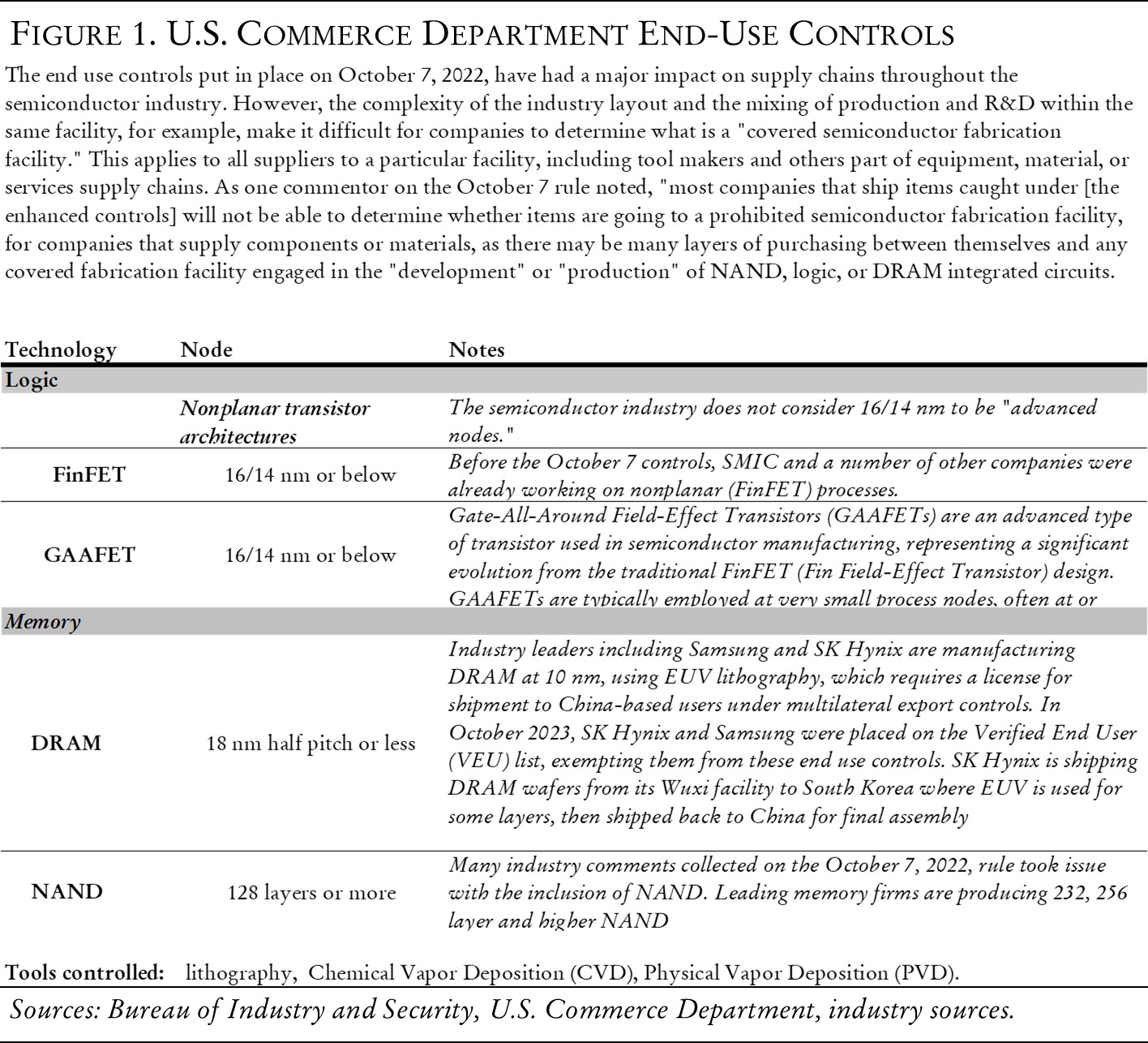
The most complex and controversial portions of the October 7, 2022, rules released by the Commerce Department9 were the end-use controls on semiconductor manufacturing tools, and on U.S. persons. The SME controls call for licensing of equipment and U.S. persons for manufacturing of logic semiconductors at 16/14 nanometers, 3-d NAND memory at 128 layers, and DRAM at 18 nanometers half pitch. The result of these controls, initially dropped unilaterally, without agreement from other key countries whose companies occupy critical portions of the SME supply chain—namely Japan and the Netherlands—was that leading U.S. toolmakers, such as Applied Materials, KLA Tencor, and Lam Research were forced to pull all their U.S. personnel from facilities in China, particularly at foundry leader SMIC, NAND memory giant YMTC, and DRAM major CXMT. In addition, the package of restrictions also imposed controls on inputs to Chinese domestic semiconductor equipment makers, in a bid to keep them from replacing foreign equipment leaders. Almost overnight, the entire Chinese domestic manufacturing and toolmaking equipment sector was thrown into a completely new era.
The October 2023 update10 to these rules has only added to the challenges Chinese semiconductor firms face. The new controls tightened thresholds around specific parameters used for some much older ASML DUV lithography tools, again moving the goalposts. The 2023 package also raised thresholds for performance of advanced GPUs that could be sold to Chinese end users, capturing a number of GPUs that global leader Nvidia had redesigned for the China market to comply with restrictions in the 2022 package.
For China’s domestic industry, the most important impact of the controls was to massively incentivize designing U.S. technology out of the semiconductor space, by both Chinese domestic and foreign firms. Prior to this, Chinese technology firms acquired and used the most advanced equipment and services available, like their peers and competitors globally. Many observers still erroneously claim that China’s Made in China 2025 strategy (announced in 2015) was a signal that Beijing wanted to go it alone in key sectors. A side-study linked to Made in China 2025 listed wildly unrealistic goals for domestic proportions of different types of semiconductor production, but this hardly represented a concerted government policy, and Chinese semiconductor companies largely ignored it. That changed in 2023. Senior Chinese semiconductor industry experts stress that domestic industry players would prefer to use the best available tools, but are now under increasing pressure to favor domestic firms and develop alternative supply chains.11
Chinese Reactions to New U.S. Controls
As the events of October 2022 began to play out in China and around the world, and Chinese industrial planners, company executives, and foreign partners assessed the damage, several critical issues emerged that will determine the future direction of China’s semiconductor industry.
First, the unilateral nature of the controls has necessitated a long and painful dialogue between the U.S. government and the governments of the Netherlands and Japan around how to align on the controls. This so-called trilateral group had been discussing controls on SME for nearly two years, but both Japan and the Netherlands preferred setting any end‑use controls at more advanced nodes, at 10 nanometers or below. When the U.S. side set the end-use controls at 16/14 nanometers, the trilateral talks broke down. U.S. officials were apparently under pressure from the Department of Defense, which had grown concerned by reports over the summer of 2022 that SMIC had been able to produce semiconductors with some layers at 7 nanometers—using existing deep ultraviolet (DUV) lithography gear and other foreign and domestic tools such as etch and deposition. This was one of many instances in which the U.S. semiconductor industry felt that the Biden administration was “moving the goalposts” around the parameters for controls on technology for Chinese end users.12
The U.S. government badly underestimated the political and industry pushback on the unilateral controls. All talk of a “trilateral agreement” was quickly dropped, and privately, U.S. officials began speaking more about “leveling the playing field” and “burden sharing.”13 Neither the Japanese nor Dutch governments wanted to be part of an agreement visibly directed at containing China’s technology ambitions, and both governments have received major pushback from their leading semiconductor firms. At the same time, neither the Japanese, the Dutch, nor the toolmaking industry were expecting memory to be included in the controls.
Memory is a very different sector than logic, highly commoditized and competitive, with no legacy nodes, requiring companies to constantly upgrade toward the most advanced processes.14 The reasons for the inclusion of memory in the 2022 controls are complex, and center on industry and administration concerns about how rapidly YMTC had been able to move up the NAND manufacturing curve. The firm was producing 128-layer NAND and moving rapidly toward more advanced processes, at 232 layers and above. U.S. concerns centered on the subsidies YMTC had benefited from under China’s National IC Investment Fund. In addition, U.S. officials cited alleged YMTC supplies of NAND memory to Entity-Listed Huawei, though these allegations have never been proven, and the imposition of extraterritorial controls of the type YMTC is alleged to have violated is in itself controversial in the industry.
Just before the controls were imposed, stories also leaked that Apple was trialing YMTC NAND memory modules for use in its iPhone and iPad product lines.15 U.S. congressional critics of China seized on this as a potential security issue, though Apple planned to use YMTC memory only for products sold in China. Cybersecurity experts also do not believe that memory, as a commodity product that is constantly being replaced with more advanced versions, would likely be used for installing some type of “back door,” making these arguments unconvincing to many industry observers.

A tentative—and probably only verbal—agreement was reached in late January 2023, with the Dutch and Japanese governments agreeing to implement some similar but not identical end-use controls of the type included in the October 7, 2022, package. However, details of the agreement suggest that, unlike the U.S. controls which included persons, Dutch and Japanese companies would be able to keep personnel on site until the completion of contracts. This put U.S. toolmakers at a major disadvantage, and has implications for the future of China’s semiconductor industry.
Finally, the October 17, 2023, controls added further challenges for Chinese semiconductor manufacturing firms, particularly foundry leader SMIC, by capturing older ASML lithography gear. Thus, by late 2023, Chinese officials responsible for industrial policy related to the sprawling semiconductor industry faced a number of short-term, medium-term, and long-term challenges.
First, how to assist leading Chinese firms like SMIC, YMTC, and CXMT to replace U.S. personnel supporting advanced tools, and slowly transition these large manufacturing operations to equipment sourced only from Chinese suppliers? The impact of the controls was already being felt at YMTC, which laid off thousands of employees in January 2023.
Second, how to provide government financial support to the industry under the new and more challenging situation? This effort has been complicated by the convulsions within the National IC Investment Fund that began in late 2021 with a corruption investigation of the fund. A sizeable number of fund executives have been arrested, including Ding Wenwu, along with industry leaders such as former Tsinghua Unigroup chairman Zhao Weiguo.16 The future role of the fund has been cast into doubt, and part of Beijing’s concern relates to the fund’s narrow focus on manufacturing and design, while not enough attention was paid to investing in the SME sector.
In late 2022 and early 2023, rumors circulated that the government was considering a 1 trillion renminbi ($141 billion) fund to bolster the sector. But leading industry figures, such as Tsinghua professor Wei Shaojun, a senior advisor to the government on semiconductor industry policy, indicated that they were not aware of such a fund being considered.17 It is likely that senior political leaders and industry planners are reluctant to announce the existence of such a fund in the current geopolitical climate and amid deteriorating relations with the United States. Their experience with such major announcements and programs, such as Made in China 2025 and the National IC Fund, has been that these initiatives become major targets of U.S. policies, and there is likely a move to avoid this happening with any future initiatives.
Hence, as of early 2024, we can now see the outlines of Beijing’s new strategy for supporting the industry, what I call China Semiconductor Industry Policy 3.0:
New top-down approach. Following the installation of a new economic team in the wake of the National People’s Congress in March 2023, there were indications that Beijing would revamp high-level oversight of the semiconductor industry. To that end, a new semiconductor industry “leading small group” was apparently established under Vice Premier Ding Xuexiang. There have been some limited references to it in Chinese media, but they were quickly removed. The new leading small group will oversee all aspects of China’s new strategy for the semiconductor industry, which has been under development for roughly the past two years.18
The new strategy is the result of internal deliberation on, and review of, past approaches to industrial policy related to semiconductors, according to industry insiders. Previously, officials determined that the scientist-led approach had not delivered much progress. The latest investigations of the National IC Fund, meanwhile, reflect concerns that the attempt to use market forces, via the fund, has also not delivered sufficient progress in key areas. Now, senior leaders feel the need for a significantly different approach. One possible new course for the sector would be to entrust oversight to a large state-owned firm or firms. Such firms are considered desirable, because they are operated by what Beijing would view as trusted officials, who will run these companies principally for the good of the country, and not to benefit themselves, as has been the case with some individuals charged with managing the National IC Investment Fund, for example.
Hence, a high-level decision may have been made that China needs a national-level SOE conglomerate to run overall semiconductor industry policy, in a manner similar to sectors like nuclear with CNNC and aerospace with casic, among others. The other state-backed companies that are regarded as being most successful in their technology areas are generally involved in national security and defense industrial sectors. Thus, if there is indeed a move to take a similar path with semiconductors in 2024, it would indicate that the Chinese leadership views the sector as increasingly important, particularly semiconductor manufacturing equipment, material supply chains, and advanced manufacturing. As of late 2023, it seemed likely that this mission could be given to one or a combination of two major state-owned conglomerates, such as CEC and/or CETC. In addition, there were also indications that most or all major semiconductor policy decision-making would be moved under the National Development and Reform Commission (NDRC).
Invest more in basic semiconductor R&D, and make R&D results available to commercial firms. There is a clear recognition that basic R&D on things like semiconductor physics, and critical technologies like light sources for advanced lithography, has not been sufficient. Part of the role of the new leading small group under Ding will likely be to better coordinate basic R&D spending and collaboration, and moving R&D from state institutions more quickly into private sector hands to develop commercial products and systems.19 In early 2023, for example, reports surfaced that the government had designated five key firms— Huawei, SMIC, YTMC, and toolmakers Naura and AMEC—to gain privileged access to government R&D.20 There has been no official confirmation of this new policy approach, but one well-placed observer noted that “the Chinese government will subsidize these companies to produce and deploy localized chipmaking tools without any funding cap, just in order to overcome US restrictions.”
Fully support open-sourced hardware architectures, specifically risc-v. Taking a longer-term view of the industry, and eager to wean Chinese firms off proprietary Western chip IP and architectures, such as x86 and Arm, Beijing is also fully supporting the development of the risc-v reduced instruction set architecture. Chinese officials, and industry leaders such as Alibaba and its chip-design arm T-Head, have embraced the risc-v approach over the past three years. Industry players in China, with government support, are working closely with the risc-v Foundation to help chart the future direction of development of the instruction set architecture.21 While the uptake of risc-v within China is progressing steadily, it will be some time before it can replace chip IP and other alternatives such as Arm, in particular.
Public-private partnerships. The most important part of the new approach to semiconductor policy will be new public-private partnerships. As Beijing has grappled with a new sectoral oversight approach, the private sector in China, likely with government encouragement, has quietly begun investing in critical R&D in areas where Chinese firms have been well behind Western counterparts. These “chokepoint technologies” have now become the target of major hybrid R&D efforts involving government research institutions and one or more private sector companies, depending on the technology in question. Telecom giant Huawei, in particular, has been active in this endeavor. A host of other Chinese private sector firms, including smart-device maker Xiaomi, have also set up funds to invest across the semiconductor supply chain.22
Huawei is by far the most important private sector driver of China’s Semiconductor Industry Policy 3.0. First and foremost, as a result of U.S. controls, Huawei has developed a close working relationship with SMIC, and specifically with SMIC’s most advanced fab, Semiconductor Manufacturing South China Corporation (SMSC), a joint venture owned by SMIC, the National IC Fund, and the Shanghai IC Fund.23 SMSC is focused on the development of advanced node processes, specifically using FinFET technology.24 According to some industry sources, SMSC has a well-developed and high-yield 12 nanometer process, and SMSC is also producing all of Huawei’s most advanced designs—including for its new smartphone and data center semiconductors—that have been adapted from designs previously used at TSMC. SMSC almost certainly has a large number of ASML DUV tools, including the advanced twinscan:2050i. In mid-2023, SMIC asked ASML to speed up 2050i deliveries. According to industry sources, the advanced ASML DUV tools that SMIC and SMSC currently have could allow SMSC to add capacity of around fifty thousand wafers per month for a 7 nanometer process, though it is not yet clear whether this could cover all of China’s advanced semiconductor requirements outside of cutting-edge smartphones.25 The SMSC facilities are also almost certainly being targeted by the U.S. Commerce Department as a result of the October 2022 end-use controls, though it is difficult to determine which facilities. See figure 2 for an analysis of which facilities may be covered.
In addition, over the past three or four years, and likely anticipating the ratcheting up of U.S. controls, Huawei has created investment vehicles like Hubble Technology Investment and quietly seeded a broad range of companies across the semiconductor supply chain, particularly in hard-technology innovation domains. Huawei is also working with a series of new foundries, including Pengxinwei (or PXW), that were established in 2021 with significant support from the Shenzhen government, likely as a future manufacturing vehicle for Huawei. PXW, however, has quickly come under U.S. government scrutiny,26 and in December 2022 was placed on the Entity List.27 PXW has targeted 28 nanometer production, but also had plans to move to 14 and 7 nanometer processes. A report by the Semiconductor Industry Association (SIA) last year alleged that Huawei was working with PXW and Fujian Jinhua (jhicc), a DRAM maker, as part of a broader effort to boost manufacturing capabilities for both logic and memory,28 presumably for Huawei consumer products and future telecommunications infrastructure. While jhicc was put on the Entity List in 2018, after allegations of IP theft from Micron, the firm has managed to continue operating, likely with injections of capital from the national and local governments as well as Huawei. Huawei’s Mate 60 phone probably used stockpiled DRAM from companies like SK Hynix,29 but Huawei needs a long-term reliable domestic supplier, hence the focus on and investment in DRAM players. It is also likely that Huawei is working with other newcomers, such as Swaysure, another DRAM player, and Qingdao Sien, a producer of power semiconductors.
In addition to working with SMIC and other existing fabs, Huawei almost certainly has its own separate effort to build a domestic-only production process. This is likely located in Shenzhen, and industry sources suggest that Huawei has already put together a 28 nanometer line and is now working toward a 14 nanometer capability. It remains unclear what the volume of production is at this facility, but it is likely small scale. Huawei is probably working with the Shanghai Integrated Circuit Research and Development Center (ICRD), along with domestic toolmakers, including SMEE, for this production line.30
The Huawei approach is complex and broad. Huawei has conducted R&D in critical areas, such as DUV and extreme ultraviolet (EUV) lithography. Chinese lithography companies appear to be years behind industry leader ASML and Japanese firms such as Nikon and Canon in these areas, making lithography one of the critical technology bottlenecks. In addition to funding many companies, including some caught up in U.S. controls, the firm is doing its own research, such as for EUV-related technologies31 that could be made available to other firms via licensing. Huawei may be attempting to become more like Samsung, an integrated device manufacturer (IDM) and foundry, which produces the most critical semiconductors for its own products. But under U.S. export controls, Huawei’s revenue, particularly for advanced smartphone handsets, has been substantially reduced, handicapping the firm’s ability to plow revenue into R&D efforts and across the many technology areas required to do advanced manufacturing.
Samsung and other IDMs also have full access to Western suites of tools. In attempting to jump-start and fund a new Chinese industrial supply chain focused on SME, Huawei thus faces an uphill battle. In late 2023, though, things were looking up for Huawei, as sales of its new Mate 60 smartphone and other advanced consumer products allowed the firm to near $100 billion in annual sales, the first uptick in revenue since 2019, even if still short of what the firm was generating before U.S. controls.32 Huawei, working with SMIC and specifically SMSC, has achieved a major breakthrough in getting back to near-cutting-edge design and manufacturing with the Mate 60, which represents a major milestone and a harbinger of the types of measures Chinese companies will take to engineer around U.S. technology restrictions. SMIC already had access to all of the tools and well-known industry techniques—such as multi-patterning using ASML DUV tools, along with capable deposition and etch gear—to produce the Kirin 9000s system on a chip (SoC) at the heart of the Mate 60, and yields are likely to go up in 2024.33
SMIC is clearly key to Huawei’s strategy of supporting fully indigenous supply chains, and not just for advanced node semiconductors. SMIC, almost certainly working with companies like Huawei, as well as toolmakers such as SMEE, AMEC, Naura, and PXX, has already created production lines free of foreign technology.34 These so-called Non-A lines will continue to use ASML or Canon lithography tools until SMEE is able to replace this equipment, and will move quickly from 40 nanometers to 28 nanometers this year, according to some observers. Given U.S. scrutiny of SMIC and other Chinese firms, there is no public acknowledgement of these efforts, making it difficult to assess progress, but industry insiders continue to suggest that aggressive timetables are being met, and there is lively discussion of the issue on Chinese-language semiconductor industry discussion groups.
Finally, Huawei is also leading the way, along with other players like Alibaba and Xiaomi, toward a risc-v future in China. Huawei is one of the twelve Chinese companies that are premium members of the risc-v Foundation, along with Alibaba, Unisoc, and other smaller players. Huawei in late 2023 released a risc-v-based microcontroller (MCU).35 Huawei’s chip design arm, HiSilicon, is reportedly working on a data-center-focused risc-v design, and also looking at using the architecture for an AI accelerator. Although Huawei is still planning to use the Arm architecture for some designs, it will pursue a mix of approaches to designing semiconductors across its business units. In addition to its Ascend line of accelerator chips that can be used for AI training, Huawei is also developing its own Maleon GPU architecture. Coupled with the Harmony mobile operating system, the firm is attempting to develop an entire non-U.S. operating system ecosystem that works across multiple devices.
Key Technologies: Lithography and EDA Tools
As U.S. export controls have driven Chinese semiconductor manufacturing firms to seek out domestic alternatives across a range of production-related technologies and materials, Beijing’s strategy for assisting the private sector is beginning to take shape, focused on a staged phasing in of domestic production processes that are largely free of Western tools. In the near term, the strategy also involves key private sector companies focusing on systems engineering approaches to get around the controls, particularly for developing advanced systems that, while not as good as Western alternatives, are good enough for many applications.
Under the new conditions, the range of technologies that Chinese firms must master has expanded considerably. Some work was being done in these areas before October 2022—such as Project 02, a government-backed research program begun more than a decade ago—but many firms likely did not believe the United States could cut off all semiconductor manufacturing technologies. Today, that possibility is dominating the thinking within the industry, and forcing both Beijing and private sector companies to develop workarounds and alternatives. Key areas include: (1) Electronic design automation (EDA) tools. (2) Lithography, etching, and deposition. These tools require vendors to work together to ensure smooth interoperability. (3) Materials, such as process gases, photoresists, and critical inputs including ABF, TGV, and TSV. (4) Chiplet design and advanced packaging technologies, including approaches such as TSMC’s Chip on Wafer on Substrate (CoWoS) to 2.5 and 3-d packaging.
Developing a strong domestic EDA tool sector is clearly one of Beijing’s priorities, and there appear to be multiple efforts underway to create alternatives to leading Western firms. As noted in my 2021 paper, Empyrean appears to be the leading Chinese EDA tool company. Empyrean claimed last year that it can fully support 7 nanometer digital processes and 5 nanometer analog processes.36 In addition, the firm is working to plug gaps between its services offerings and those of Western leaders like Cadence and Synopsis. Huawei has also been developing EDA tools37 for some time, ever since its chip design arm HiSilicon was added to the Entity List in 2020. In early 2023, a senior company official noted that Huawei, in cooperation with domestic EDA companies, had succeeded in “basically realizing the localization of EDA tools above 14nm.”
Prior to U.S. export controls on Huawei in 2019 and 2020, HiSilicon had full access to EDA tools from global leaders Cadence, Synopsis, and Mentor, as well as semiconductor IP from Arm. Also in 2019, probably just before Huawei and HiSilicon were placed on the Entity List, the firms purchased a large number of EDA licenses from the leading Western firms for ten years, and 7 nanometer was then supported by the tools.38 Hence western EDA tools were likely used to design the Kirin 9000s, as the original design of the Kirin 9000 was done before 2019. Since that time, Huawei has been working on its own EDA tool suite. Although it still has access to foreign EDA tools, it does not have access to software updates and support, driving the firm to develop an alternative EDA ecosystem for the long term. While other Chinese design firms not on the U.S. Commerce Department Entity List continue to have access to Western EDA tools, they are more are likely over time to switch to domestic alternatives as these software ecosystems mature.
The current strategy for developing semiconductor manufacturing production appears to include both short- and longer-term goals. In the short term, leading domestic foundry SMIC, with the support of key players in the industry, including all the domestic toolmakers and others such as Huawei, is attempting to establish 40 and 28 nanometer production lines free of U.S. equipment. In the near term, however, the lithography component will likely still include ASML DUV immersion lithography gear, which China’s lithography leader SMEE is working to improve for use at 28 nanometers and below. Complicating this effort are U.S. and Dutch controls that took effect on September 1, 2023, and January 1, 2024. Significantly, U.S. controls included in the October 17, 2023, update now include restrictions on the twinscan 19XX series of equipment, which TSMC used for some critical layers at 7 nanometers before it had access to EUV systems. SMIC did the same thing with these and more advanced ASML systems in 2022 and 2023, which in part triggered the U.S. decision to raise end-use controls to 16/14 nanometers in the October 2022 controls. SMIC’s N+1 and N+2 processes, used at the SMSC fabs, are continuing to improve the technology base for this type of production, while attempting to improve commercial yields. All the Kirin 9000s and Ascend 9XX series of chips for the Huawei Mate 60 and AI applications are coming from SMSC’s FinFET processes, which they have been able to keep going despite the October 2022 end-use controls.
In late 2023, there were indications that SMEE had been able to produce a workable and potentially commercial 28 nanometer DUV immersion lithography tool, based on social media reports that were later changed and then removed but picked up by Western media.39 SMEE’s state-owned backers, the Shanghai Zhangjiang Group (ZJ Group) in a December 19 post on a verified social media account, which was later removed, noted that, “As the only company in China to have mastered lithography technology, SMEE has successfully developed a 28 nm lithography machine.” The story of how SMEE has achieved this level is complex, and likely includes some assistance from players such as Huawei. Some Chinese media stories suggested that, in 2021, Huawei had attempted to poach sizeable numbers of SMEE engineers for its own lithography effort40 but was persuaded by Chinese government officials to change course and collaborate with SMEE. The Chinese government also likely asked SMEE to benchmark its new 28 nanometer DUV system against similar ASML equipment, specifically the NXT:2000i.41 The SMEE system—the SSA800A—is now likely part of a fully domestic production line that is being tested and certified.
The SMEE lithography efforts that resulted in the SSA800 series, which has i-line, KrF, Arf, and Arfi product lines, were heavily backed by a major Chinese megaproject that was part of the fifteen-year plan for science and technology development released in 2006. The sub-project, called Project 02, was launched back in 2008, and named “The Project of Manufacturing Complete Sets of Technology for Very Large Scale Integrated Circuits.” Because of the backing of Project 02, SMEE has benefitted from government efforts to coordinate suppliers for SMEE equipment,42 but this effort has been quite slow to gel into something more viable. Other key government R&D institutions such as the Chinese Academy of Sciences, a number of top-flight Chinese universities such as Tsinghua, and key national laboratories have assisted in the effort. In addition, Huawei’s investment vehicle, Hubble Technology, has also invested in one of the firms backing the effort and supplying SMEE: the Beijing Keyi Hongyuan Optoelectronics Technology Co., which is providing the excimer laser at the heart of the DUV system. It is likely that the U.S. controls on Huawei in 2019 and 2020, and the Biden administration’s unprecedented package of controls in October 2022, galvanized the entire effort.
China’s other key toolmakers, as noted in my 2021 report, had for some time been able to obtain only small shares of key market segments such as etch, deposition, and metrology. One of the most important impacts of the October 2022 controls, however, was to force the industry into boosting collaboration and innovation. This has happened quickly according to industry insiders, who note that there is now a high level of integration among the leading toolmakers and the foundries. Some key players, such as Naura, which makes etch, deposition, and cleaning tools, were already cutting into the market share of leading Western firms before October 2022, but the company has made major gains since.43 In particular, Naura equipment has replaced many U.S. toolmakers at facilities subject to U.S. end-use controls, such as YMTC. In early January 2023, the firm noted that its revenue for that year was projected to jump by 42–57 percent. Competitor Advanced Micro-Fabrication Equipment China (AMEC) also forecast major gains for 2023 revenues, citing increased demand from domestic fabs. YMTC, in particular, has engaged in new and much deeper levels of cooperation with companies including Naura and AMEC, along with other firms in the supply chain, in part to enlist help with obtaining replacement parts, and to ensure that domestic players can improve capabilities and replace foreign toolmakers over time, likely sooner rather than later in some key areas. Foreign toolmakers are expressing increasing concern that the improvement in the quality of the products of domestic toolmakers will also eventually enable them to compete outside of China, putting even more pressure on sales, revenue, and R&D budgets needed to maintain leading positions.44
Once the 40 and 28 nanometer lines have been validated, SMIC and other players in the industry will turn to a similar process for 14/10 nanometer production, almost certainly at SMSC,45 probably sometime in 2025–26. It is possible that, given the SMEE breakthrough with the SSA800, this system could be used down to 7 nanometers, but it remains unclear how quickly this will happen and whether SMEE can manufacture multiple commercial versions of the SSA800. All of these efforts will also likely include ensuring compatibility with the use of EDA tools developed by Huawei and other smaller players, in order to ensure that the entire design and manufacturing process will be largely free of export-controllable U.S. and allied technologies.46 If the goal is to move from 40 to 28, and then to 14/10 and 7 nanometer production lines, this will take a major effort involving all the key suppliers: even though the Chinese toolmakers claim their equipment is capable of 14 or even 7 nanometers, the key customers, particularly SMIC, will still have to validate these tools under high-volume production. As of late 2023, this process appeared to be part of SMIC’s effort to have a fully domestic 14 nanometer line by the end of 2024.
But while the DUV efforts are likely to bear fruit in the short term, they are not a long-term solution. Looking out two to three years, even if SMIC and other foundries can leverage SMEE DUV gear for production at 7 nanometers, getting to more advanced nodes will require extreme ultraviolet (EUV) lithography systems, a niche where only ASML has been able to develop commercial systems. In China, there are now likely at least two and maybe three separate efforts to develop EUV systems, in some cases using different approaches to producing the 13 nanometer light that is used in ASML systems. These efforts involve collaboration, which has probably increased recently under the new semiconductor industry policy thrust. One effort is being led by the Changchun Institute of Optics, Fine Mechanics, and Physics (ciomp) and the Chinese Academy of Sciences.47 Another likely involves Huawei. In addition, the Shanghai Integrated Circuit Research and Development Center (ICRD) is doing advanced work in this area.
Chinese researchers are also looking at a novel approach called steady‑state micro-bunching (SSMB) EUV. In a 2022 paper published in the Chinese journal Acta Physica Sinica, Tsinghua University researchers proposed a design using SSMB that includes a system the size of a football field. Its light source supplies several dozen EUV machines all working simultaneously.48 This approach appears quite far from any level of commercial application, but over the longer term it could become important.
It is likely Huawei is also leading efforts to tackle some EUV technology problems. This may not be a completely separate effort from the others, as there are almost certainly areas where the different R&D efforts come together in various forms of collaboration. For example, developing the appropriate types of photoresists are critical for EUV lithography, and there have been a number of patents filed for an EUV photoresist, for example from Shanghai Sinyang.49 Chinese semiconductor manufacturers are overwhelmingly reliant on Japanese suppliers for photoresists, and in the wake of Japan’s alignment with U.S. export controls, fears have grown within the industry that material exports could also come under pressure. A November 2022 report from a domestic Chinese investment firm claimed that, for less advanced traditional photoresists, around 30 percent were provided by domestic suppliers, while for DUV KrF processes, this dropped to 10 percent; the ratio of domestically supplied photoresists for advanced Arf DUV and EUV was under 2 percent.50
Hence, in addition to the light source and scanner system itself, there appear to be multiple, coordinated efforts to establish a complete ecosystem for a production process that would use EUV. Furthermore, it is likely that EDA tool capabilities targeting 3–5 nanometer process nodes are being developed.
While China’s domestic firms lag behind global leaders like ASML, Nikon, and Canon on lithography hardware, there are also efforts to close the gap on a critical software part of these systems, called computational lithography. Chinese firms are attempting to develop better computational lithography capabilities, and in 2022, a company called Yuwei Optical claimed to have independently developed computational optimal proximity correction (OPC) software, which it said was being tested and verified.51 This will likely be a multiyear process and require continued access to ASML equipment and maintenance, and improvements from China’s domestic toolmakers and materials producers across a spectrum of technologies.
When it comes to design and packaging, some Chinese firms are using chiplet design already, which is a design approach that integrates chips produced using different processes on one substrate, along with advanced packaging technologies, including 2.5- and 3-d packaging. Biren’s BR 100 GPU, for example, uses two chiplets, manufactured—before the October Entity Listing of Biren—on a TSMC 7 nanometer process. In addition, Huawei is pursing R&D for designs using chiplets. Packaging is now becoming a key part of overall production, with back-end packaging being designed into the entire production process, from EDA tools, to integration of IP from companies such as ARM, to 3-d packaging designs that enable greater functionality with a mix of semiconductors at different levels of complexity. Huawei, in collaboration with domestic packaging leaders such as JCET and Tongfu, is working on its own EDA tools as part of this process.52 R&D efforts are also being pursued under the National Natural Science Foundation of China, which last year released the 2023 project guide for the Scientific Basics Major Research Plan for Integrated Chip Frontier Technology, which included support for research on 2.5- and 3-d packaging.53
Closely related to packaging are materials, such as photoresists, substrates, and process gases. This is where Chinese firms remain well behind global leaders in Japan and South Korea. Japan, in particular, dominates the supply of photoresists—just four Japanese firms (Fujifilm, Shin-Etsu, JR, and TOK) account for over 70 percent of the global market—and films such as Ajinomoto Build-up Film (ABF), a type of insulating film used in the production of high-performance semiconductors, such as CPUs. It is essential for electrical insulation and helps to ensure the efficient flow of electrons within the chip. So far, there have been no efforts to control these types of materials, but Chinese companies are concerned that materials such as substrates could eventually be restricted, and are working to develop domestic alternatives.54 There are numerous Chinese photoresist players, such as Shanghai Sinyang, Xuzhou Bokang, Jingrui, Nata Opto-electronic Material, and Red Avenue, that are at various stages of developing, producing, and validating photoresists for use with KrF, ArF, and ArFi lithography. Sinyang, for example, in addition to developing EUV photoresist, is expected to complete facilities for KrF, ArF, and i-line markets by the end of 2025 and will start production later in 2026 with a capacity of around five hundred tons. Photoresists have a very high set of requirements due to their impact on yield, and the validation process for domestic sources of photoresists for advanced node processes is likely to be long.
Looking Ahead
As of early 2024, the future of China’s semiconductor industry remains hanging in the balance. Many technical hurdles must be overcome in order to build ecosystems that will allow high-end design firms such as Huawei, Alibaba, and others to design and manufacture advanced chips free of concerns around U.S. export controls. Given the number of different technology areas that are under intense development in China, it also remains to be seen when individual technologies or groups of key technologies will mature to the point of enabling scaled commercial production for a particular manufacturing-supply-chain element.
Looking ahead, some Chinese domestic design firms can be expected to retain access to foundry services outside of China, but for some subsectors, like GPUs, there is likely to be further tightening of U.S. export controls that will cutoff more Chinese GPU start-ups from access to TSMC, among others. There will be some key signposts along the way. For example, 2025 is likely to be a big year for Huawei in particular, given the firm’s unique position within China’s semiconductor and IT sectors, deploying design, production, and commercial prowess across a range of subsectors. Especially if SMIC is able to get to some type of 5 nanometer process, it looks increasingly likely that Huawei will have a full lineup of largely domestically produced telecommunications, AI, server, computer desktop, smartpad, and smartphone semiconductors by 2025.
As part of this evolution, it is expected that SMIC will also have significantly more capacity by 2025 at 5/6/7 nanometers for other customers such as Alibaba’s T-Head, GPU leaders Biren Technology and Moore Threads, and other domestic design firms. SMSC will almost certainly prioritize advanced manufacturing capacity for technology leaders, including Huawei and other critical players such as firms developing GPUs to eventually replace Western products from Nvidia, AMD, and Intel. Much of the likely performance gains here are expected to come not so much from reduced feature size, but from improvements in design and packaging—Huawei’s Mate 60 in this sense was a preview of things to come.
The manufacturing roadmap looks something like this: over the next three years, domestic toolmakers aim to put together commercial production lines at 28, 14, 7, and even 5 nanometers that scale. This will see key foundries, such as SMIC, primarily, and Hua Hong, use existing foreign—ASML, Canon, and Nikon—DUV equipment, and some domestic DUV tools from SMEE. The challenge here will be to keep foreign equipment going when access to spare parts and software upgrades may be difficult.
In addition, work will continue steadily on the various EUV projects, including building up a cadre of engineers, managers, and supply-chain specialists to begin developing sustainable ecosystems for EUV systems development and deployment later in the decade. In the most optimistic scenario, according to some industry watchers, progress on EUV means that SMIC could get its hands on a prototype system to begin testing in 2025, but this scenario is much more optimistic than other industry assessments.55
For many applications, including 5G and training large language models (LLMs), the advanced DUV capability at SMIC and Hua Hong should be able to satisfy a growing portion of the domestic demand for advanced GPUs. At the same time, some Chinese companies that remain off the U.S. Entity List, like ZTE, Lenovo, Xiaomi, and others, will still be able to design and manufacture semiconductors using overseas foundry services such as TSMC. China will have a complex hybrid semiconductor manufacturing landscape, with key players like memory makers YMTC and CXMT hobbled by lack of access to cutting-edge tools, but still capable of producing useable memory, while others like Huawei will be relying on SMIC, first with a mix of foreign and domestic, and then domestic-only, tool production lines.
During this period, Chinese firms across the supply chain will be making significant gains, particularly for EDA tools for advanced nodes, materials such as photoresists and process gases, and newer areas such as substrates, chiplet design, and proprietary advanced 2.5- and 3-d packaging capacity.
Assuming Beijing’s new semiconductor industry policy produces significant gains for technologies like DUV to keep China’s design and manufacturing industry afloat, the period from 2027–30 will likely see some significant success in moving to commercial production—meaning high-volume manufacturing (HVM)—using more advanced systems with some type of EUV technology ecosystem. In addition, Chinese packaging firms and foundries such as SMIC and Hua Hong will also have moved up the value chain and mastered a number of advanced packaging techniques, including mostly proprietary approaches.
The advances made by domestic foundries and other key players in the Chinese semiconductor manufacturing supply chain will gradually produce two separate but linked manufacturing ecosystems: China domestic and global mainstream. Factors shaping this trend include the pace and scope of the development of alternatives, the willingness of Chinese toolmakers and other ecosystem players to export and support manufacturing outside of China, and the scope and enforcement of U.S. government efforts to control access to technology inputs, particularly around the flow of talent, especially engineering and managerial know-how. At the end of the day, however, the U.S. approach to export controls—the belief that preventing Chinese firms from accessing key U.S. and allied-country technology will prevent Chinese companies from doing certain things—will founder on the rocks of reality. The underlying problem of U.S. export controls is that we are dealing with applied science, and there is no single path to achieving technological performance levels, only many different, albeit difficult paths. Chinese firms will find the paths that work well enough to continue to drive innovation. A similar process is already at play with Huawei’s HarmonyOS.56 As the developer ecosystem around the platform grows, other domestic and foreign companies are recognizing that the scale of the deployment of the Chinese-developed OS now merits attention and the resources needed to develop applications on the platform.
Major Challenges Remain
At Davos in January 2024, Intel CEO Pat Gelsinger asserted that China faced a “10 year gap and a sustainable 10 year gap,” given all the export control policies that have been implemented by various countries.57 But in an X (the platform formerly known as Twitter) poll run by one tech industry observer, most people disagreed with Gelsinger’s estimate.
Nevertheless, the headwinds facing the Chinese semiconductor industry remain strong, as the Biden administration and subsequent U.S. administrations are likely to continue to ratchet up export controls around key technologies across various semiconductor supply chains, and pursue more multilateral approaches to controls specifically for China. One significant complication for SMIC, SMSC, Huawei, and other companies that are working more collaboratively to develop alternative supply chains for advanced manufacturing will be continued U.S. government efforts to target any company that American officials may judge to be associated with the Huawei effort. The SIA report that outlined Huawei’s influence over the semiconductor industry and alleged collaboration between companies that received investments from Hubble, for example, could lead U.S. officials to place other companies on the Entity List, not for past or current actions, but because of the potential to supply Huawei in the future. This is already the case with PXW, for example. Such a move is a novel use of export controls, and another example of U.S. officials “moving the goal posts.”58 One former Commerce official, Kevin Wolf, noted that it was impossible to know whether firms like PXW are violating U.S. regulations without more detailed information.59 It remains unclear why SIA, which represents leading U.S. front-end manufacturing firms and toolmakers, is focused on the potential future impact of Huawei’s investments in China’s semiconductor supply chain and which firms Huawei could use for future sourcing of some semiconductors.60 The impact of the U.S. approach to export controls in general, and on Huawei in particular, will likely mean that major U.S. and other foreign toolmakers are increasingly squeezed out of the Chinese market—U.S., Dutch, and Japanese toolmakers are already among the biggest losers from export control policies targeting Chinese semiconductor firms like SMIC, YMTC, and CXMT.
In addition, early in 2024, there were indications that the Biden administration planned to add one or more Chinese organizations involved in developing risc-v-based solutions to the Entity List.61 It was not clear whether this was the start of a major effort targeting the risc-v ecosystem, and there is likely to be a lot of opposition from the industry. One industry executive called the move “absolutely silly,” and Beijing will likely react strongly to any move to include open-source technologies in the U.S.-China technology competition, which have previously been outside U.S. export controls. American officials in early 2024 were also considering tightening export licensing around companies like Huawei and Inspur, and adding more Chinese technology firms to the Entity List. The U.S. government is also likely to continue to put pressure on the Dutch and Japanese governments,62 along with, potentially, the Korean government, around exports of DUV lithography and other systems, as well as spare parts and service to specific Chinese end users. These measures are likely to draw a strong reaction from Beijing, which last year added critical materials such as gallium and germanium, widely used in the semiconductor industry, to a list requiring licensing for export. So far, Beijing has not restricted exports of these and other materials, but 2024 may see some moves in this direction, creating further disruptions in semiconductor supply chains.
Another major wild card will be the willingness and ability of the Dutch and Japanese governments, working with their semiconductor toolmakers, all major national champions, to align with evolving U.S. controls on tool exports to Chinese facilities. Both governments appear reluctant to fully align with U.S. preferences, particularly around controlling less advanced equipment, such as immersion DUV. Both governments also remain concerned about potential Chinese retaliation.63 At least for the near term, companies in the Netherlands and Japan, as well as South Korea, are likely to continue to provide some level of support, including spare parts, software updates, and servicing by company personnel, at facilities in China.
Senior leaders such as Vice Premier Ding Xuexiang and Premier Li Qiang, along with Chinese government officials at MIIT and NDRC overseeing the sector, will continue to look for new ways to boost the domestic industry in the coming year, including subsidies, favorable policies, and enhancing the existing new structures at the top, such as the leading small group. At the same time, Chinese authorities appear to be in the process of determining the optimal role for a large state-owned enterprise in overseeing elements of domestic industry development.
On the whole, the Chinese semiconductor landscape has become much more complex and diverse, with many players, entrants, and new types of investment, and we should expect to see more announcements of domestic technology breakthroughs. But the real measures of success in overcoming the challenges the industry faces will be the production of new products with largely domestic supply chains, like the Mate 60, new GPUs from companies like Biren and Moore Threads, and the willingness of other Chinese companies to eventually move to domestic alternatives.
This article originally appeared in American Affairs Volume VIII, Number 1 (Spring 2024): 29–52.
Notes
The author wishes to thank, among others, @tphuang, a close industry observer, for his contributions to the drafting of this article, through regular and detailed discussions over the past several years. He also would like to thank a number of other unnamed industry insiders who provided significant context and helped the author understand the major new directions of semiconductor industry policy and private sector engagement in China.
1 Paul Triolo, “The Future of China’s Semiconductor Industry,” American Affairs 5, no. 1 (Spring 2021): 90–113.
2 Bureau of Industry and Security, U.S. Department of Commerce, “Implementation of Additional Export Controls: Certain Advanced Computing and Semiconductor Manufacturing Items; Supercomputer and Semiconductor End Use; Entity List Modification,” Federal Register 87, no. 196 (October 13, 2022): 62186–215.
3 Paul Triolo, “Your Phones and Cars Aren’t Going to Work the Same after New U.S. Rules on Selling Chips to China,” China Project, October 25, 2022.
4 Bob Johnson, “The Road to Terrabuck Opportunities and Speedbumps along the Way” (presentation at semicon iss, Half Moon Bay, January 2023). Author attended.
5 See, for example, Paul Triolo, “Technology Crossroads: Innovation in China’s Telecommunications and High-Performance Computer Sectors Threatened by US Stranglehold on Semiconductors,” Asian Security 19, no. 2 (2023): 143–58.
6 Antony J. Blinken, “The Administration’s Approach to the People’s Republic of China,” U.S. Department of State (speech presented at the George Washington University, Washington, D.C., May 26, 2022).
7 Jake Sullivan, “Remarks by National Security Advisor Jake Sullivan on the Biden-Harris Administration’s National Security Strategy,” White House, October 13, 2022.
8 Jake Sullivan, “Remarks by National Security Advisor Jake Sullivan at the Special Competitive Studies Project Global Emerging Technologies Summit,” White House, September 16, 2022.
9 Bureau of Industry and Security, “Implementation of Additional Export Controls.”
10 Bureau of Industry and Security “Public Information on Export Controls Imposed on Advanced Computing and Semiconductor Manufacturing Items to The People’s Republic of China (PRC) in 2020 and 2023,” U.S. Department of Commerce, November 6, 2023.
11 Author discussions with Chinese semiconductor industry experts, Track 2 dialogue, National Committee for U.S. China Relations, 2018–23.
12 See Paul Triolo, “The Industry View of U.S. Export Controls: Moving the Goalposts,” Wire China, January 14, 2024.
13 Author discussions with U.S. industry representatives, 2022–23.
14 Paul Triolo, “Memory Test: The U.S.-China Chip War Escalates,” China Project, November 11, 2022.
15 Cheng Ting-Fang, Lauly Li, and Yifan Yu, “Apple Freezes Plan to use China’s YMTC Chips amid Political Pressure,” Nikkei Asia, October 17, 2022.
16 See, for example, Shen Xinmei, “Former Chip Guru at Tsinghua Unigroup Pleads Guilty in Corruption Trial after Beijing’s Anti-Graft Push,” South China Morning Post, September 23, 2023.
17 See, for example, Frederic Nyame, “China vs US Tech War, China to Use New Strategy,” GizChina, December 31, 2022.
18 Author discussions with Chinese industry experts in Beijing, Shanghai, and Shenzhen, 2022–23.
19 See, for example, “Strengthen the Basic Capacity Building of Semiconductors and Light Up the ‘Lighthouse’ of Semiconductor Self-Reliance and Self-improvement Development,” Bulletin of the Chinese Academy of Sciences, February 16, 2023.
20 Qianer Liu, “China Gives Chipmakers New Powers to Guide Industry Recovery,” Financial Times, March 20, 2023.
21 Sunny Cheung, “Examining China’s Grand Strategy for Risc-v,” Jamestown Foundation, December 15, 2023.
22 Yu Cong and Han Wei, “Xiaomi-Backed Fund Raises $388 Million More for Chip Investment,” Caixin Global, March 8, 2023.
23 Semiconductor Manufacturing International Corporation, Disclosure and Connected Transactions in Relation to Proposed Capital Contribution and Deemed Disposal of Equity Interest in SMIC and Notice of Extraordinary General Meeting (Hong Kong: Hong Kong Exchanges and Clearing, 2018).
24 The Irony is that SMIC/SMSC’s FinFET process development probably “would have gone nowhere if Huawei had not lost access to TSMC” according to a knowledgeable industry insider.
25 Tphuang (@tphuang), “Another IC Note Before Shanghai Motor Show,” X Post, April 16, 2023.
26 Bloomberg News, “Secretive Chip Startup May Help Huawei Circumvent US Sanctions,” Bloomberg, October 5, 2022.
27 Bureau of Industry and Security, Department of Commerce, “Additions and Revisions to the Entity List and Conforming Removal from the Unverified List,” Federal Register 87, no.242 (December 19, 2022): 77505–18.
28 Bloomberg News, “Secretive Chip Startup May Help Huawei Circumvent US Sanctions.”
29 Mark Tyson, “Huawei Allegedly Used Years-Old SK Hynix ‘Ghost RAM’ in Mate 60 Pro,” Tom’s Hardware, September 15, 2023.
30 Discussions with industry observers, December 2023–January 2024.
31 Judy Lin, “Huawei Confirms Breakthrough in EUV Lithography Process Optimization,” DigiTimes, December 26, 2022.
32 Juan Pedro Tomas, “Huawei Reported its Revenues in 2023 Would Expand by Nearly 9% Year-on-Year,” RCRWireless, January 2, 2024.
33 Paul Triolo, “What Huawei’s New Mate 60 Means for China, the U.S. and the Global Tech Industry,” Wire China, October 1, 2023.
34 Cheng Ting-fang and Sunksuke Tabeta, “China’s Chip Industry Fights to Survive U.S. Tech Crackdown,” Nikkei Asia, November 30, 2022.
35 Rodney Chan, “Huawei Chip Design Arm HiSilicon Launches Risc-v MCUs,” DigiTimes, January 16, 2024.
36 Misha Lu, “Chinese EDA Champion Empyrean Can Now ‘Fully Support’ 7nm; Sees 1Q23 Sales Growth,” DigiTimes, May 22, 2023.
37 David Kirton, Josh Horwitz, and Brenda Goh, “Huawei Makes Breakthroughs in Design Tools for 14nm Chips—Media,” Reuters, March 24, 2023.
38 Judy Lin, “How Did Huawei Design Its Kirin 9000s Chip without American EDA Tools?” DigiTimes, October 6, 2023.
39 Debby Wu and Sarah Zheng, “Chinese Chip Gear Leader Achieves Key Breakthrough, Backer Says,” Bloomberg, December 20, 2023.
40 “Many Shanghai Companies Complain about Huawei, Almost All Employees Received Calls except the General Manager,” Ifeng, July 27, 2020.
41 “Did China’s ‘28nm Lithography Machine’ Miss Its Deadline Again? Where Is It Stuck?,” Zhiku, accessed January 27, 2024.
42 “Increase the Lithography Field? Huawei Hubble Invests in Keyi Hongyuan,” EEworld, June 4, 2021.
43 Che Pan, “Tech War: Chinese Chip-Tool Giant Naura Forecasts Surge in 2023 Sales on Strong Local Demand amid US Export Controls,” South China Morning Post, January 16, 2024.
44 Author discussions with industry companies, 2022–24.
45 SMIC’s efforts to achieve more advanced process are being driven primarily via a joint venture it established in 2010, SMSC. The joint venture was originally funded by SMIC with 50.1 percent and the remainder provided by the National IC Fund and Shanghai IC Fund, respectively. SMSC has built and operated a 300 millimeter wafer fabrication facility in Shanghai to produce advanced integrated circuits (ICs), specifically focusing on 14 nanometer and below technologies.
46 “Huawei Makes Breakthroughs in Design Tools for 14nm Chips,” Reuters, March 24, 2023.
47 Chai Kewei, et al., “Detection of Carbon Contamination in EUV Multilayer Mirrors Based on Secondary Electrons,” Vacuum 221 (March 2024).
48 Tang Chuan-Xiang and Deng Xiu-Jie, “Steady-State Micro-Bunching Accelerator Light Source,” Acta Physica Sinica 71, no.15 (2022): 152901–15.
49 Application number CN117270320A, “A MOFs Photoresist Product and its Preparation Method” China National Intellectual Property Administration, accessed January 14, 2024.
50 Gabby Chen, “JW Insights: Chinese Fabs Face Risks of Photoresists Export Controls by Japan and Support is Given to More Substitutive Makers,” ijiwei, March 14.
51 Gabby Chen, “China’s Software Startup YWO Successfully Develops OPC Software for Computational Lithography,” ijiwei, November 23, 2023.
52 See, for example, “Huawei Chiplet Expert Exchange Summary,” Jiuyangongshe, February 3, 2023.
53 National Natural Science Foundation of China, Announcement on the Publication of the 2023 Project Guide for the Major Research Plan on the Scientific Foundations of Cutting-edge Integrated Chip Technology (Beijing: National Natural Science Foundation of China, 2023).
54 Rodney Chan, “China Urged to Step Up Photoresist Self-Sufficiency,” DigiTimes, August 1, 2023.
55 For example, a Gartner presentation at semicon iss 2024, attended by the author, put progress on EUV systems much further out in the decade.
56 See, for example, Iris Deng, “McDonald’s China Pushes Development of Native Apps Based on HarmonyOS, as Adoption of Huawei’s Mobile Operating System Accelerates,” South China Morning Post, December 7, 2023.
57 Kevin Xu (@kevinsxu), “At Davos, Pat Gelsinger Said He Believes China’s Lag in Advanced Chip Manufacturing,” X Post, January 17, 2023.
58 Triolo, “The Industry View of U.S. Export Controls: Moving the Goalposts.”
59 Bloomberg News, “Key Taiwan Tech Firms Helping Huawei with China Chip Plants,” Bloomberg, October 2, 2023.
60 Media stories called out Huawei’s investments and interests in other industry players “a secret network,” but SIA suggested that much of what was in its report was known from public sources. See Ian King and Debby Wu, “Huawei Building Secret Network for Chips, Trade Group Warns,” Bloomberg, August 22, 2023.
61 Don Clark and Ana Swanson, “The Next Front in the U.S.-China Battle over Chips,” New York Times, January 10, 2024.
62 See, for example, Jack Simpson, “ASML Halts Hi-Tech Chip-Making Exports to China Reportedly after US Request,” Guardian, January 2, 2024.
63 For more on this, see for example, Paul Triolo (@pstAsiatech), “Recent Announcements from the Dutch Government,” X post, March 12, 2023.
